Bo Joel Svensson
blog (dot) joel (dot) svensson (at) gmail (dot) com
| Last edited |
June 3 - 2020 |
| Board compatibility |
TE0736-03 |
| Tested Vivado versions |
2019.2.1 |
Preface to version 2020.0
Back in 2015 or 2016 me and a colleague at the time wrote the first version of this guide on how to "get started" with OpenCL HLS on the Zynq platform. We wrote it because we struggled immensely to get anywhere with this and once that we did get something to work, we felt that it was worth sharing. There must be someone else, somewhere out there going through the same struggle with this. I think that I can safely say that yes, someone else was struggling in the same way because I have never before been contacted so many times by people with questions about anything else I've ever been part of writing.
Years have passed since the writing of this and I have been doing other things for a while. Haven't really touched FPGAs or the Zynq very much at all in quite a while. So, I want to see how relevant this document still is and also see if I can update or improve it in some way. Step one in this process is to try to go through it myself using contemporary versions of the tooling.
The Zynq-board that I use is still the Trenz Zynqberry equipped with a Zynq 7010. Board-files for these boards can be found in the reference designs that Trenz provides on their website, look here for info and here for actual reference designs. The board files can be found in a subdirectory.
An older version of this guide can be found on researchgate. I have no idea how much has changed. That will become clear while going through the steps and writing this updated document.
Thanks for reading! I hope this document will be easy to follow and will help someone get started with FPGA programming. Thank you!
Disclaimer
All content provided in this document is for informational purposes only. The authors makes no guarantees as to the accuracy or completeness of any information within this document.
The authors will not be liable for any errors or omissions in this information nor for the availability of this information. The authors will not be liable for any losses, injuries, or damages from the display or use of this information.
Introduction
This document attempts to provide a complete walk through of the entire OpenCL HLS work flow using Xilinx Vivado. That is, it will all be about interacting with the various GUIs.
This document is work in progress and new versions will be posted as we refine the procedure and gain a deeper understanding of all the details.
All feedback, hints, tips, corrections and explanations of details we are vague upon, would be greatly appreciated!
Initial setup
Board files should be copied from a reference design that can be downloaded here (if you are using the ZynqBerry). The interesting files are located in the subdirectory named board_files within the reference design archive. The subdirectories within board_files should be copied to a directory in your Vivado installation. I installed Vivado under a directory called opt within my home directory. So, in my case I copy the contents of board_files to directory:
~/opt/tools/Xilinx/Vivado/2019.2/data/boards/board_files
If your starting point is a fresh install of Vivado on a Linux machine there are some additional steps that must be taken. There is a script that installs some "cable_drivers" and sets some udev rules located in the following directory:
~/opt/tools/Xilinx/Vivado/2019.2/data/xicom/cable_drivers/lin64/install_script/install_drivers
This script should be run (sudo ./install_drivers). Then source the vivado settings, this updates the path variables in your current shell so that all the necessary tools can be found.
source ./opt/tools/Xilinx/Vivado/2019.2/.settings64-Vivado.sh
Guide structure
This guide is split into three parts that goes through: first writing a simple OpenCL program and synthesizing it using Vivado HLS, second designing a system (in Vivado) that interfaces the hardware generated by HLS in step 1 with the processing system and the memory system in the Zynq chip, finally we show how to develop software (in the SDK) for the processing system that starts computations in the OpenCL generated hardware.
Part 1: Vivado HLS and OpenCL
In this section we develop an OpenCL program for vector addition (vadd). This vadd computation is given pointers to three vectors (arrays), two inputs and one output, and performs element wise addition of the inputs into the output.
Creating a Vivado HLS project
Start Vivado_hls and create project using the steps outlined below. If you have sourced the Vivado settings, Vivado_hls can be started by the command vivado_hls in the same console.
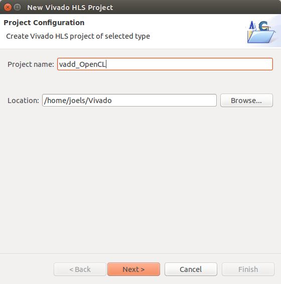
step1: Create a project and name it “vadd_OpenCL”.
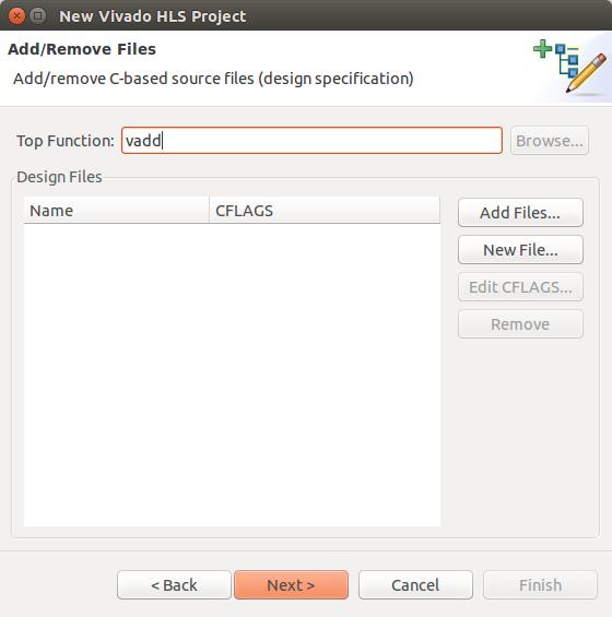
step2: Now you are asked to provide a name for the top level function. This is the function that specifies the interface to the generated hardware. Name the top level function (vadd).
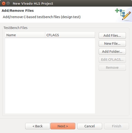
step3: We are not adding a testbench file.
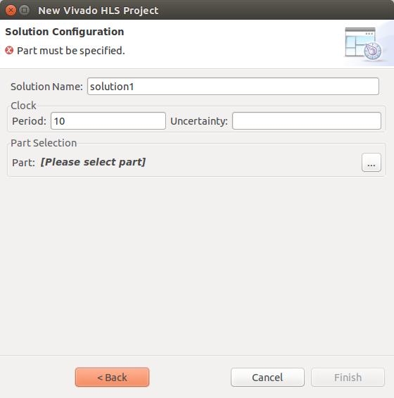
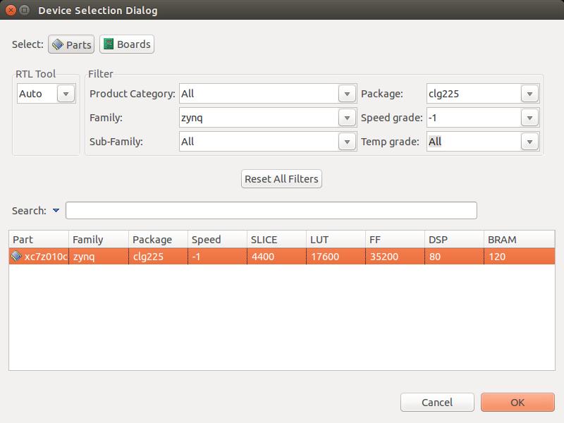
step4: Now it is time to configure the solution details. We can leave the solution name unchanged (“solution1”) and then we select the device:
Family: Zynq
Package: clg225
Speed grade: -1
These steps are of course very specific to the particular FPGA that your development board is equipped with. Looking up the actual values for your situation can most likely be done in the datasheets associated with your board. But if you have a the very same ZynqBerry as I do, the choice to pick is xc7z010clg225-1 that is suitable for the TE0726-03 version ZynqBerry.
Now project configuration is done and we can hit finish and enter into the development environment.
Writing a simple OpenCL kernel
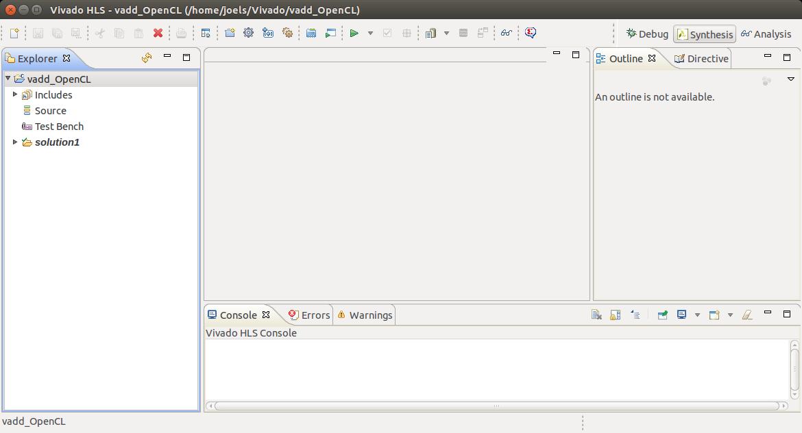
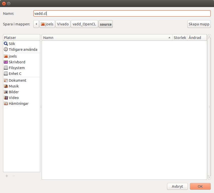
The example kernel used in this guide is very simple and is outlined in total below. Add a new source file to the project. Right click “source” in the Explorer under “vadd_OpenCL” and select “New file”. Name the file “vadd.cl”. The file extension is important “.cl”.
#include <clc.h>

__kernel void __attribute__ ((reqd_work_group_size(128,1,1)))
vadd( __global int *a, __global int *b, __global int *c) {
  int i = get_global_id(0);

  c[i] = a[i] + b[i];
}
After creating the new file type in the OpenCL code as above.
Synthesize the OpenCL code
After writing the OpenCL, synthesis and exporting the IP remains in order to conclude the part of the work that takes place in vivado_hls. If the code has been entered correctly this should go through synthesis without problems. Hit the green “synthesis” button in the toolbar.

As the synthesis finishes a post synthesis report is brought up.
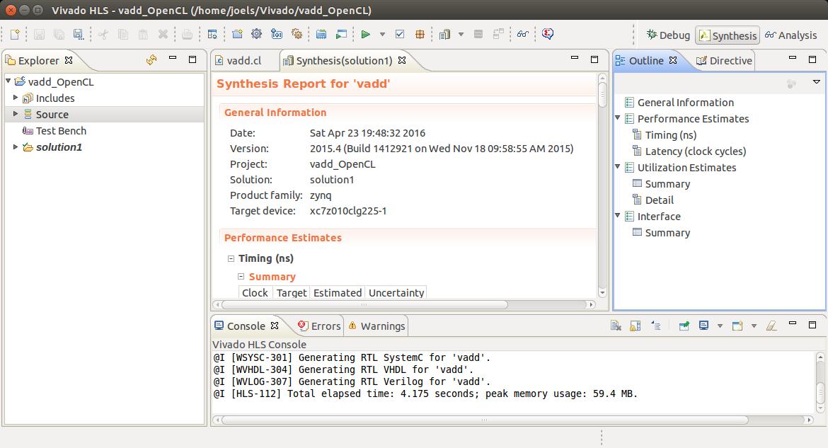
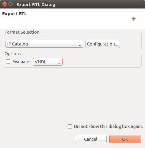
Now export the generated hardware description into the IP catalog. This step makes our vadd hardware unit available for use in Vivado. Click the “Export RTL” button in the toolbar.

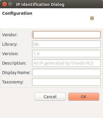
In the “Export RTL” dialog we choose “IP Catalog” and VHDL as the desired language. One can also provide identification details using “Configuration” button but we leave these settings unchanged.
We are now done with vivado_hls and will start up Vivado.
Programming Interface Generated by HLS
After synthesizing hardware from the OpenCL code new directories appeared called “impl” and “syn” containing VHDL code. Within one of these files we find information that is important to keep in mind later when writing the software that interfaces with the generated hardware, this information will be used later. The information we seek, is located in the “vadd_control_s_axi.vhd” file and shows the layout of the memory mapped interface for communication with the vadd hardware unit:
-- ------------------------Address Info-------------------
-- 0x00 : Control signals
--        bit 0  - ap_start (Read/Write/COH)
--        bit 1  - ap_done (Read/COR)
--        bit 2  - ap_idle (Read)
--        bit 3  - ap_ready (Read)
--        bit 7  - auto_restart (Read/Write)
--        others - reserved
-- 0x04 : Global Interrupt Enable Register
--        bit 0  - Global Interrupt Enable (Read/Write)
--        others - reserved
-- 0x08 : IP Interrupt Enable Register (Read/Write)
--        bit 0  - Channel 0 (ap_done)
--        bit 1  - Channel 1 (ap_ready)
--        others - reserved
-- 0x0c : IP Interrupt Status Register (Read/TOW)
--        bit 0  - Channel 0 (ap_done)
--        bit 1  - Channel 1 (ap_ready)
--        others - reserved
-- 0x10 : Data signal of group_id_x
--        bit 31~0 - group_id_x[31:0] (Read/Write)
-- 0x14 : reserved
-- 0x18 : Data signal of group_id_y
--        bit 31~0 - group_id_y[31:0] (Read/Write)
-- 0x1c : reserved
-- 0x20 : Data signal of group_id_z
--        bit 31~0 - group_id_z[31:0] (Read/Write)
-- 0x24 : reserved
-- 0x28 : Data signal of global_offset_x
--        bit 31~0 - global_offset_x[31:0] (Read/Write)
-- 0x2c : reserved
-- 0x30 : Data signal of global_offset_y
--        bit 31~0 - global_offset_y[31:0] (Read/Write)
-- 0x34 : reserved
-- 0x38 : Data signal of global_offset_z
--        bit 31~0 - global_offset_z[31:0] (Read/Write)
-- 0x3c : reserved
-- 0x40 : Data signal of a
--        bit 31~0 - a[31:0] (Read/Write)
-- 0x44 : reserved
-- 0x48 : Data signal of b
--        bit 31~0 - b[31:0] (Read/Write)
-- 0x4c : reserved
-- 0x50 : Data signal of c
--        bit 31~0 - c[31:0] (Read/Write)
-- 0x54 : reserved
-- (SC = Self Clear, COR = Clear on Read, TOW = Toggle on Write, COH = Clear on Handshake)
This gives us the “offsets” from some base address to where each of the register used by the vadd hardware is located. Later, in vivado, a complementary step will provide us with the base address.
The directly important pieces of information here is the control register, the group_id registers and the a,b and c data registers.
Control: using this register we can start computations in the vadd hardware unit and also poll for the done signal.
Group id: group_id_x, group_id_y, group_id_z specifies a three dimensional workgroup id. Since the OpenCL kernel we use is meant for one dimensional “NDRanges” only group_id_x is of importance. This value (group_id_x) is changed between invocations of vadd if the data we operate upon is larger than what can be computed by one workgroup instance (the only valid value for the others is zero).
Argument pointers: pointer to memory where the vadd hardware can fetch and store data should be written to the a,b,c register.
Concluding part 1
So far everything seems to work very much the same as "years ago". I did notice that there were some new clickboxes in the Export RTL dialogs, but ignoring those seems fine so far. If it turns out to be a problem I will edit this.
Part 2: Vivado
This section presents step by step instructions on how to integrate the OpenCL kernel IP-block designed earlier into a Zynq base system.
Creating a Vivado project
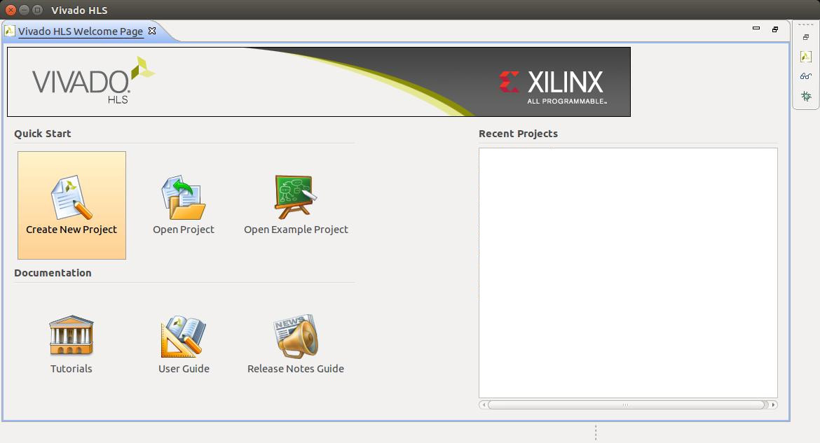
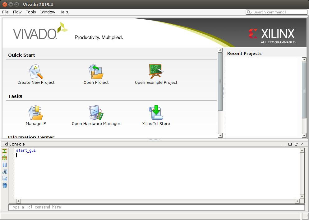
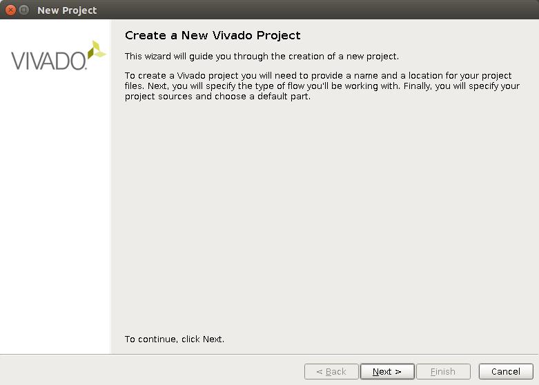
Begin by starting Vivado, this is done with the command vivado in the console that you sourced the Vivado settings in. This presents you with the view shown in the figure below. Select “Create New Project” and click “Next”.
The GUI that starts up for project creation had some cosmetic changes since last time I used Vivado but when it comes functionality it seems the same.
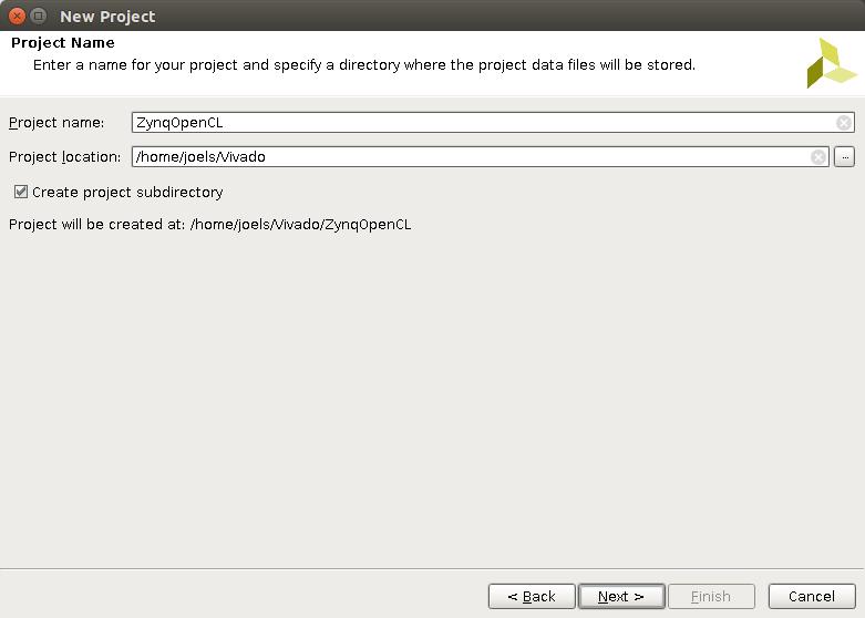
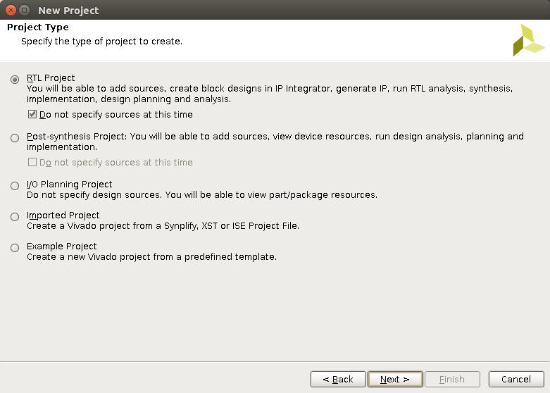
Choose a name and location for the project, in this case “ZynqOpenCL” and a directory called “Vivado”. Click “Next”. In the next window select “RTL Project” and check “Do not specify sources..”. This part of the procedure is shown in the figures below.
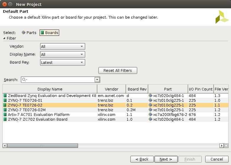
Now it is time to select the “Default Part” to use as target platform. Click “Boards”. If the steps in the section about initial setup have been performed there should be an options for different versions of the zynqberry board. Select the suitable board then click “Next” and then “Finish’
In the 2019 version of Vivado this part of the GUI has been extended with pictures of boards. But the functionality of the GUI is the same.
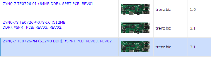
Since I have the TE0726-03 version of the Zynqberry i selected the board that is highlighted in the picture above.
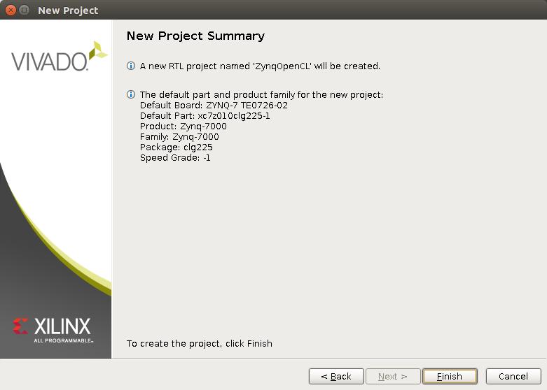
This concludes the project configuration procedure.
Designing the system
Now we have entered Vivado and are presented with a “Project Manager” view, a “Project Summary” and the “Flow Navigator”.
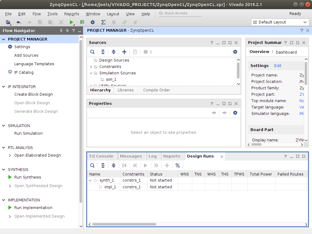
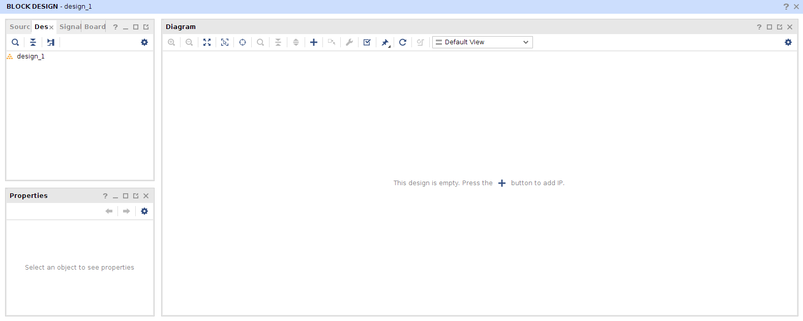
In the Flow Navigator select “Create Block Design” located under the heading "IP INTEGRATOR". The default name “design_1” is fine and we can keep it and just hit “OK”. This should bring up a “Block Diagram View” as is shown below.
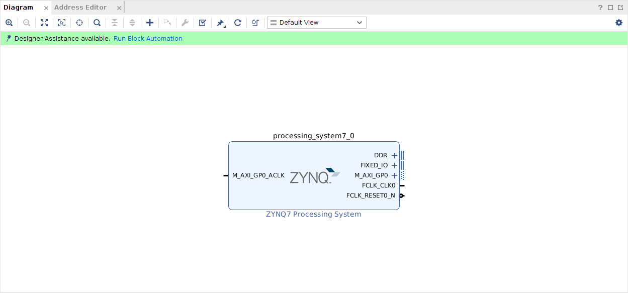
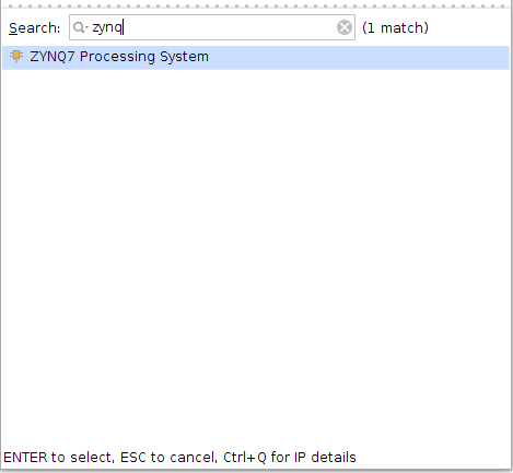
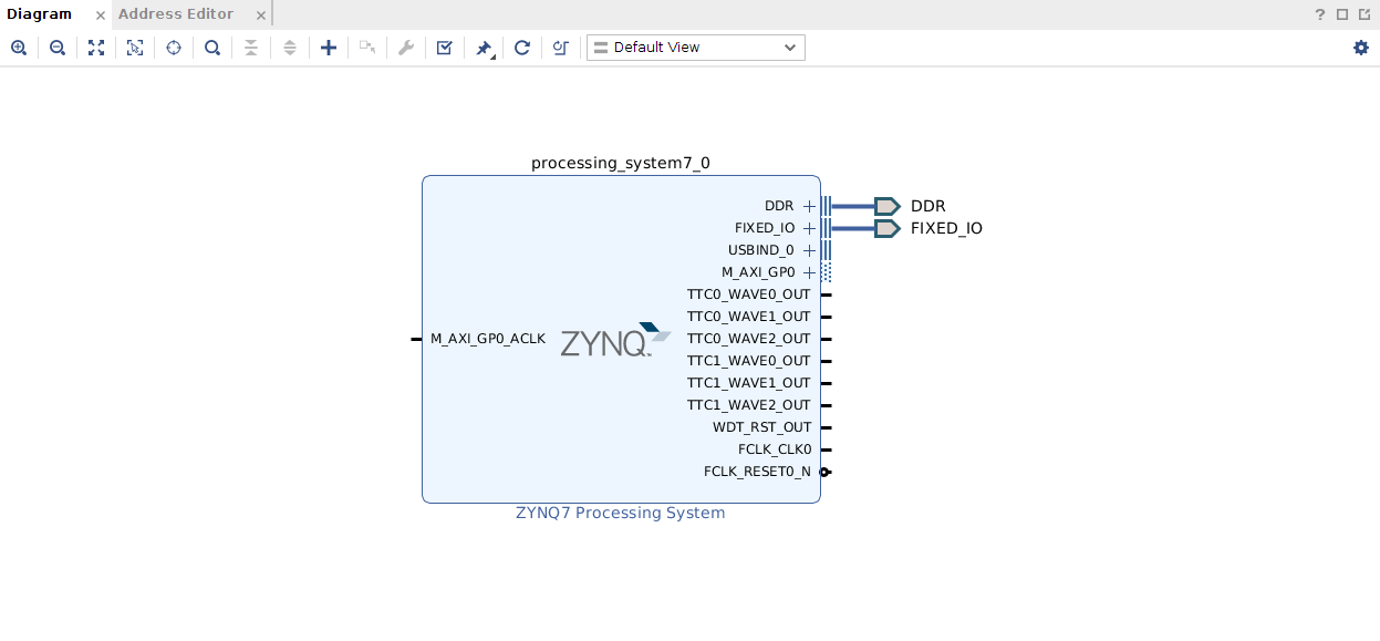
In the Diagram view “design_1” we click the add IP button. The shape of this button should now be shown in the middle of the diagram view. Click “add IP” and enter “zynq” into the search field. Select the “ZYNQ7 Processing System”. IP blocks can later be added by right clicking in the diagram area and selecting "Add IP" in the menu that pops up.
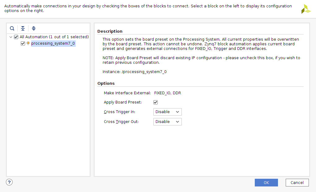
The diagram view should now contain a Zynq processing system as shown in the figure below. Note that there is a “Run Block Automation” link within the block diagram at this point. Hit this link and mark “All Automation” and then click Ok. The block automation dialog is shown in figure 19.
After allowing the block automation for the processing system to apply the default settings, the block diagram should look as in the figure below.
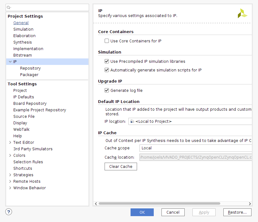
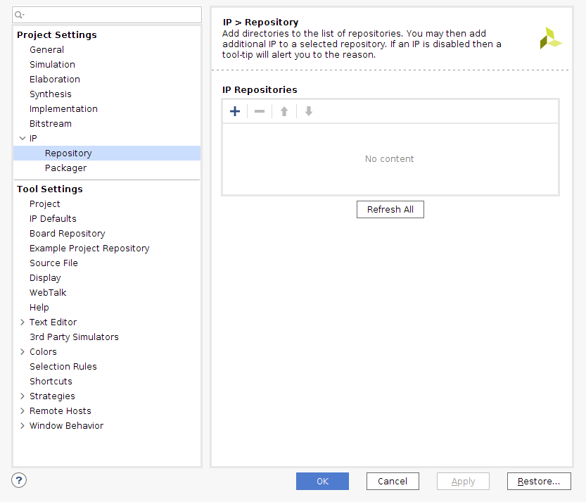
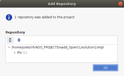
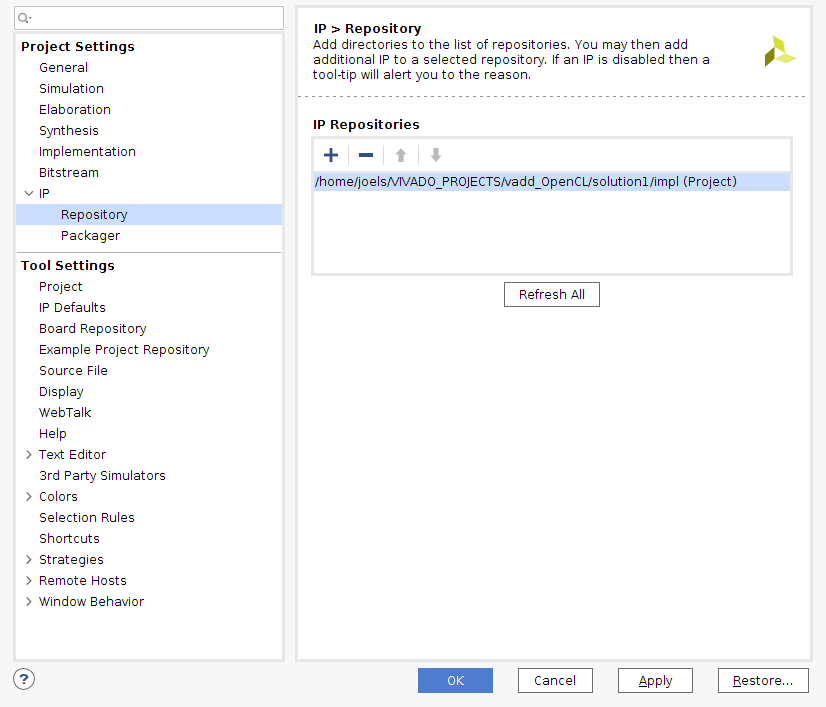
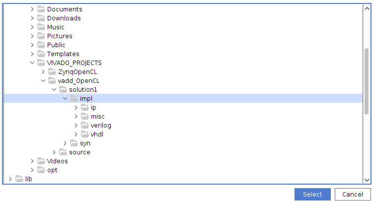
Now it is time to add the vadd IP block to the design but before doing that we need to point out to Vivado where that IP can be found. Find the “IP settings” by right clicking in the diagram area of the GUI. . Then click the “Repository Manager” tab and the plus (+) symbol. Find the “impl” directory of the vadd_OpenCL vivado_hls project and click select. This process is outlined in pictures below.
Clicking “Select” should bring up the “Add Repository” dialog. Just click “OK” and then we are back to the list of IP Repositories, but now augmented with our recently added IP. Click “OK”.
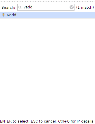
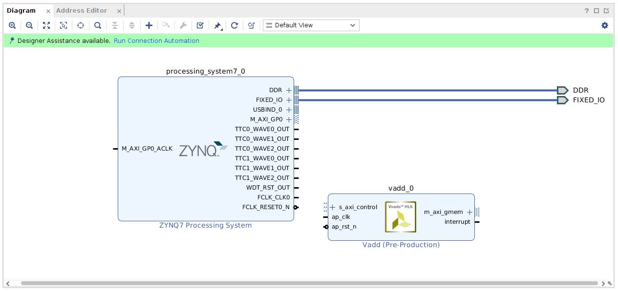
With the IP repository configured we can add the vadd IP to the design. Right click and select “Add IP” within the diagram view. Type “vadd” in the search field and the “Vadd” IP should appear in the list window. Select it.
After adding the Vadd IP the block Diagram should look as in figure 26. Now we need to connect the Vadd unit to the processing system but in order to that we need to go into the processing system block and reconfigure it. If you look at the Vadd_0 unit it has a “s_axi_control” interface and a “m_axi_gmem” interface. These interfaces needs to be connected (as well as the clock and reset). Luckily much of this connecting can be done for us automatically, if only we configure the processing system block correctly.
Double click on the ZYNQ7 Processing system in the in the diagram view. This should bring up a view of the internals of the processing system as below:
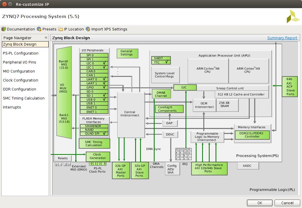
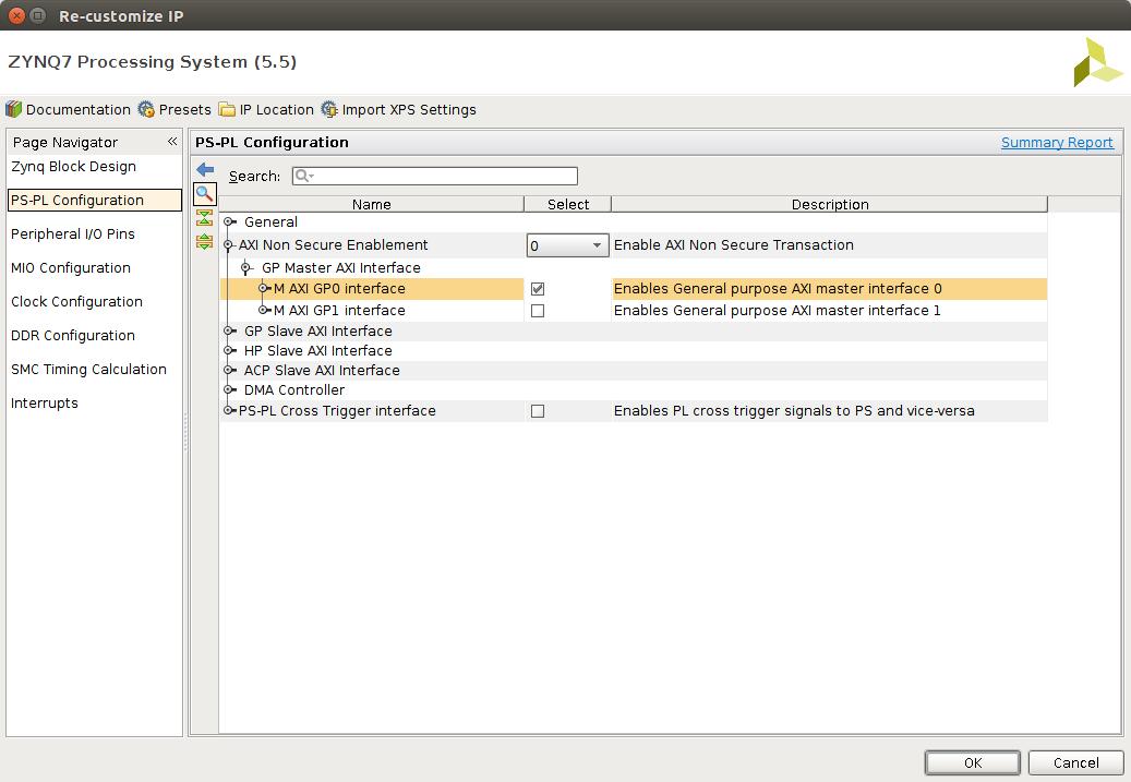
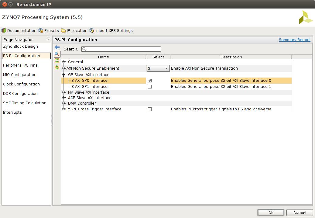
There are two interfaces that needs to be configured inside the processing system. the “32b GP AXI Master Ports” and the “32b GP AXI Slave Ports”. Double click on the Master ports and configure according to the left picture below. Then do the same for the Slave ports and the right picture.
All of this is very similar to the old document. There seems to be a difference in that the AXI master port was already enabled. This is most likely due to some update in the board files.
When this configuration of the processing system is completed the ZYNQ Processing System in the diagram view should show the newly added interfaces.
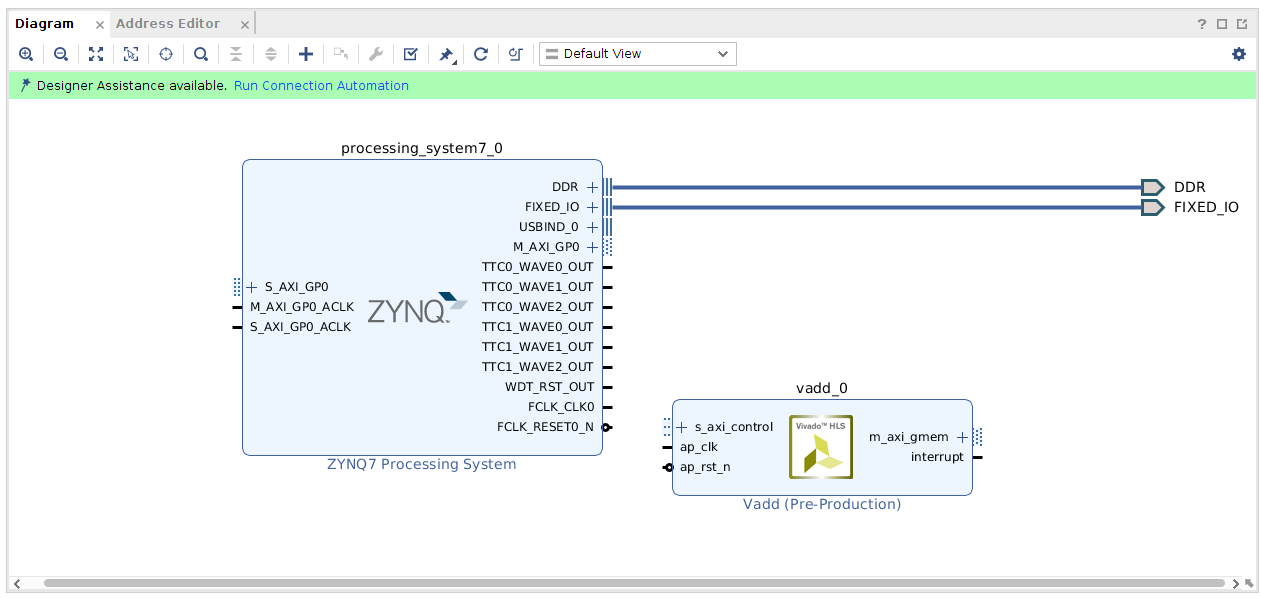
Most important here is to note that this change makes the “Run Connection Automation” link to appear at the top of the block diagram view. Actually, This time the link has been there a while. This is because the AXI master interface was already activated and could have been auto-connected. I think it is better to wait until now, when the slave interface is also activated before running the automation though.
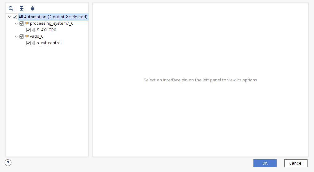
Click the "Run Connection Automation" link and make the following selections:
At this point the diagram view should look similar to the picture below. Notice how two AXI interconnects have been automatically added to the design and connects to the processing system and to the vadd unit. One of these interfaces connect to the control port on the vadd unit and is used to program the vadd unit control registers. The other interface is used by the vadd unit for memory accesses.
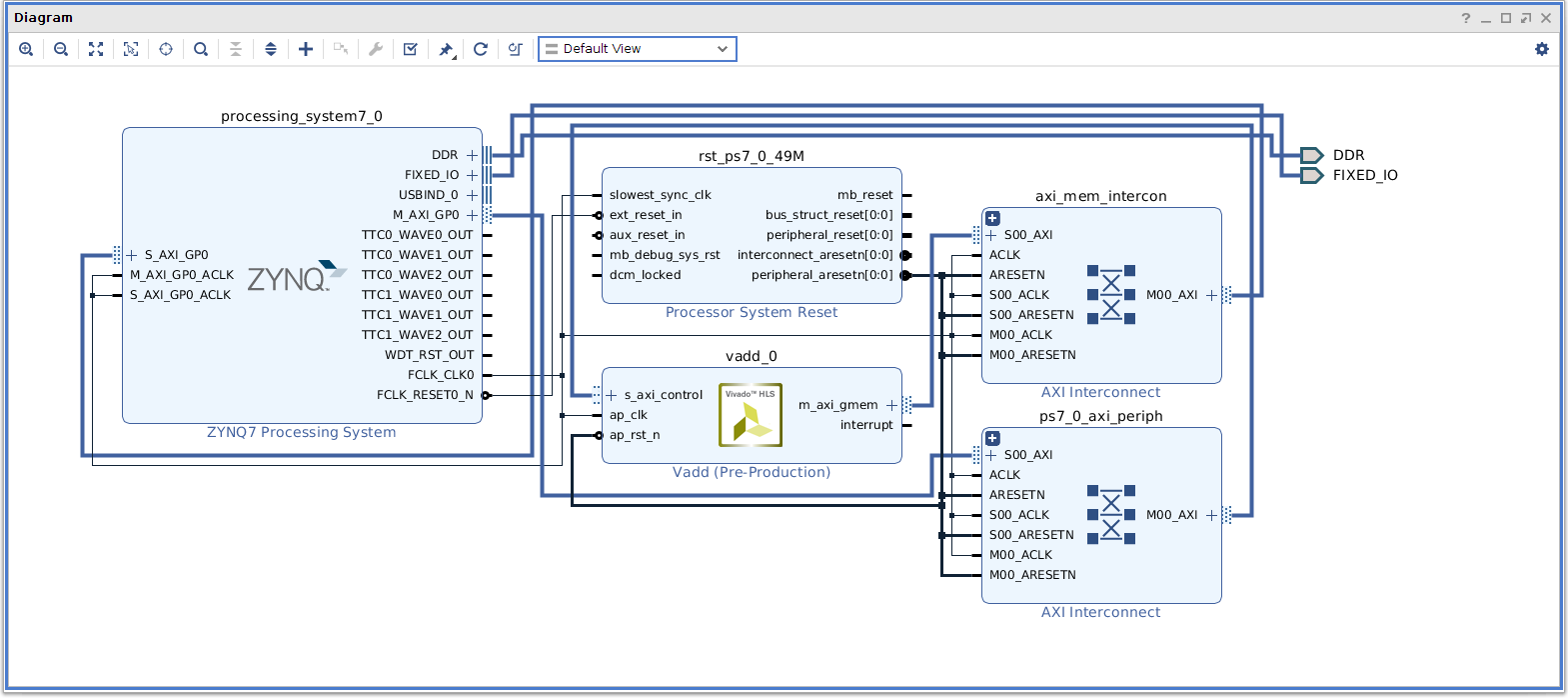
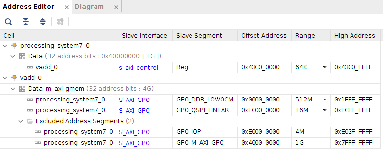
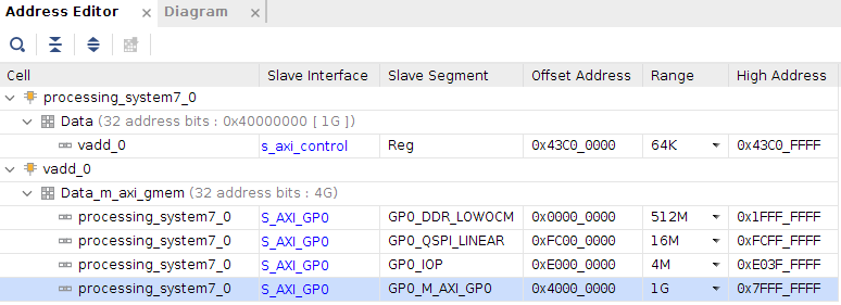
At this stage the design is mostly complete. We do, however, need to go into the “Address editor” and perform some small tweaks. Within the Address editor some address ranges are listed as excluded, we need to set these as included.
Now it is time to go through the process that in the end results in a bitstream that we can use to program the Zynq FPGA. This procedure is outlined below, in text, and following this in pictures:
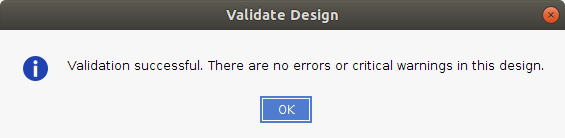
Validate the design: In the tools menu, click Validate design. This should finish with a message saying “Validation successful”.
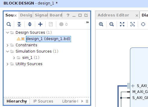
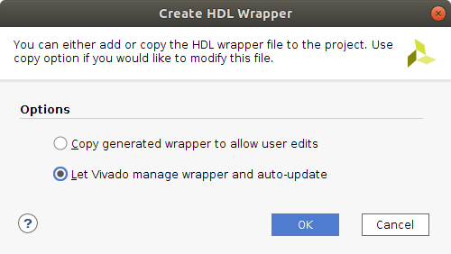
Create HDL wrappers: This is done in the sources window by right clicking on “design_1” and selecting “Create HDL Wrappers”.
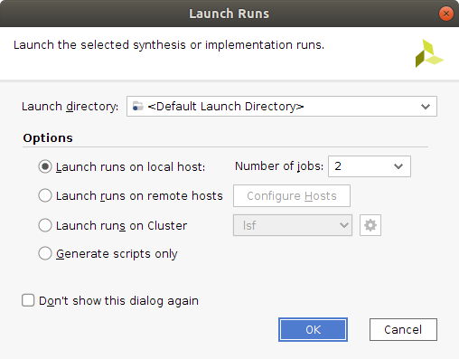
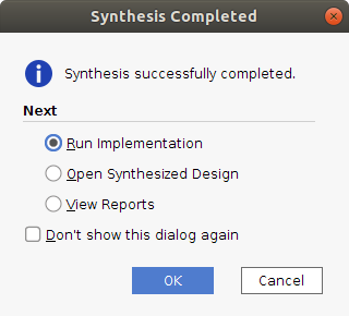
Save and run synthesis: In the flow navigator under synthesis, click run synthesis.
Synthesis completed: In this dialog choose “Run Implementation”.
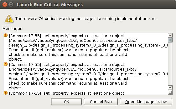
Implementation completes: Potentially reporting a great number of critical warnings. Fortunately these can be ignored. One should however check where the warnings come from. If there are warnings directly in relation to the IP you developed yourself it may be important.
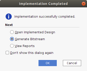
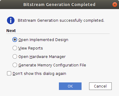
Implementation Completed dialog: Choose “Generate Bitstream”.
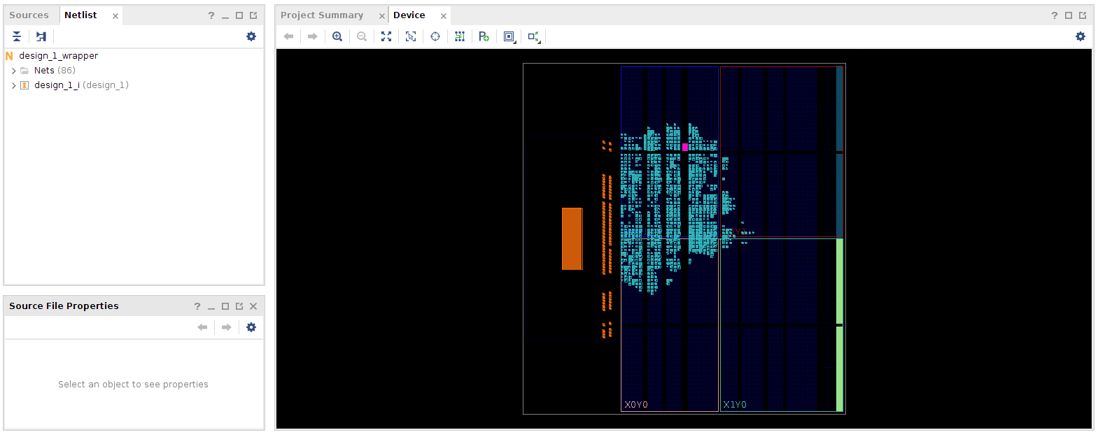
After generation of bitstream one can take a look at the implemented design.
Once you start the synthesis (and your computer is anything like mine), your system will be working very hard and use up a lot of memory for quite a long time and can as result become very unresponsive.
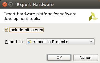
Now "Export" the hardware. Go to the FILE menu and select EXPORT followed by export hardware.
Here things start to look quite different compared to back in the old days! I cannot find any Launch SDK. There is this thing called "Launch Vitis" under the TOOLS menu. I think this may be the replacement! Clicking Launch Vitis starts something called the Vitis IDE (which is based on eclipse).
Before going into the work with the software for the ARM processor lets review some important details from the address editor.
Important details from the Address Editor
Before going into the part of the guide that looks at Vitis, we want to point out some details from the Address Editor. Make a note of the address mentioned for the s_axi_control. In this case this address is 0x43C00000. It is on this address and onwards that the control registers for the vadd hardware unit is mapped into the address space.
Part 3: Vitis
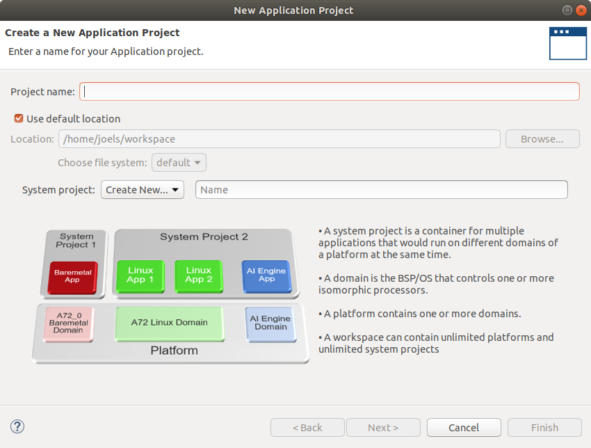
When Vitis has started (after launching it from the Tools menu in Vivado) we are presented with a welcome screen. Select "Create Application Project".
This brings up a "New application project" dialog where we name out project. I named mine "HelloOpenCL".
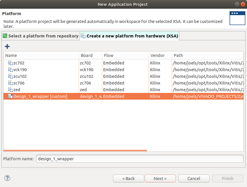
Clicking next brings up a dialog where we can chose between a platform from repository or a new platform from hardware (XSA). We want to create a new platform hardware.
Click the + in the "Create a new platform from hardware (XSA)" tab and locate the design_1_wrapper.xsa in the Vivado project directory. Then click next.
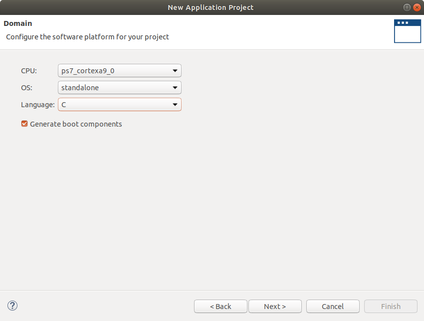
Next up is a dialog where you can "configure the software platform" the default settings are fine. A standalone project (bare-meta) in the C-language. So just click next on that.
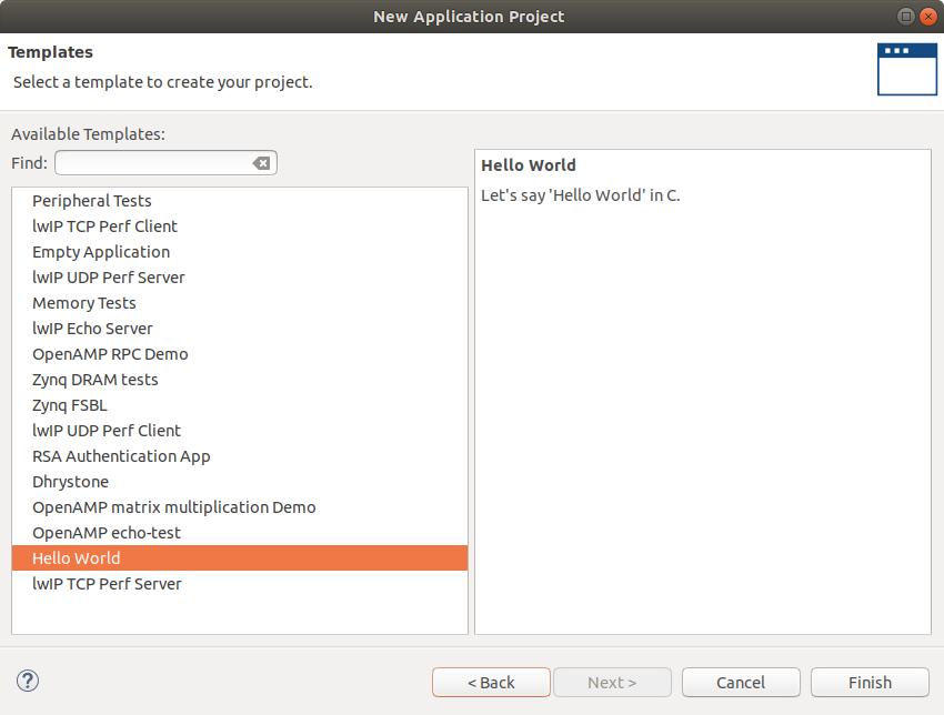
When the template selection dialog pops up we select "hello world" and click finish.
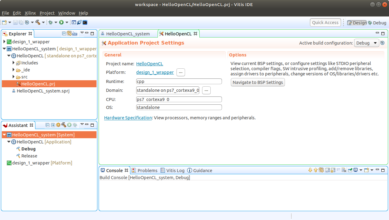
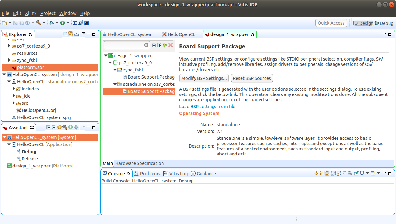
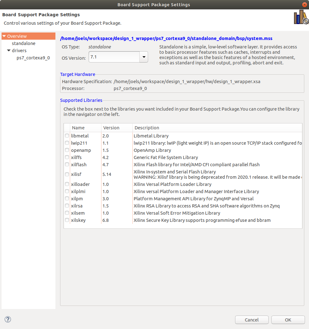
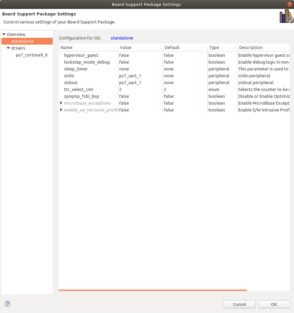
The application project settings that now are visible also look good per default as does the contents in the Board support package. It used to be that some changes had to be applied in the board support package so that IO was directed at the correct uart for the board. But this seems to have been fixed in the newer files from Trenz. Remember that many of these steps are little bit specific to the board you use! so always double check these things.
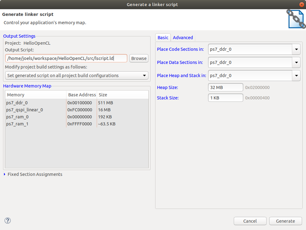
Next go to the Xilinx menu and generate a linker script. I generate one for 32MB of Heap and 1KB of stack. That is enough for this program.
Before going into the code that runs vadd, we can experiment a little with the hello world code from the template. You find the source in the "Explorer" to the left in the GUI under "HelloOpenCL" and under the src directory.
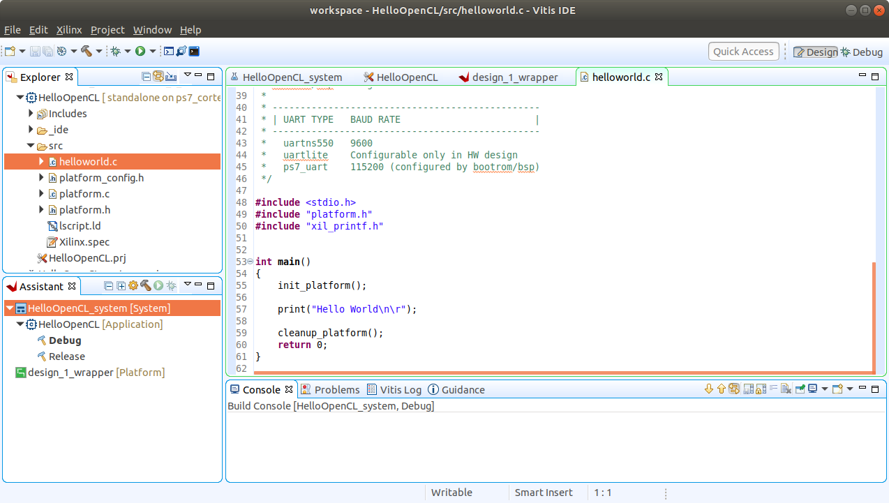
The hello world template provided in vitis has a bug (it seems). It tries to include a file called "xil_printf.h" which does not seem to exist and rather one should include "xil_io.h". Now I also tweaked the hello world program to output "hello world" repeatedly in a loop, just for fun.
Including "xil_printf.h" used to be the way to go earlier. So it may be that this particular template just has not been updated. I will look into this a bit more later. If you happen to know some details about this just send me an email. I would much appreciate it.
#include <stdio.h>
#include "platform.h"
//#include "xil_printf.h"
#include "xil_io.h"

int main()
{
    init_platform();

    while (1) {
        print("Hello World\n\r");
    }

    cleanup_platform();
    return 0;
}
Build the software using CTRL+B.
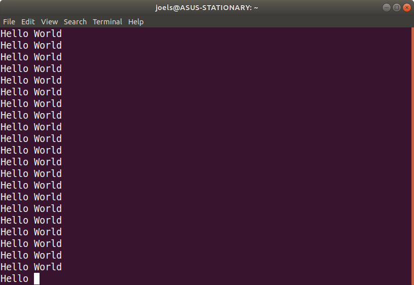
To start a debug session of the software right click debug in the "Assistant" to the left in the GUI, select debug and launch on hardware.
I use the screen command as a serial terminal and connect to the development board using the command screen /dev/ttyUSB0 115200. The picture below shows the output when debugging the program on hardware.
Example code that starts the vadd kernel
Now it is time to write the C code that talks to the vadd unit. Edit the “helloworld.c” file in the “HelloOpenCL” project and replace the contents with the code below.
#include <stdlib.h>
#include "platform.h"
#include "xil_io.h"
#include "xil_mmu.h"
#include "xil_cache.h"
#include "xil_cache_l.h"
volatile char *control = (volatile char*)0x43C00000;
volatile int *wg_x = (volatile int*)0x43C00010;
volatile int *wg_y = (volatile int*)0x43C00018;
volatile int *wg_z = (volatile int*)0x43C00020;
volatile int *o_x = (volatile int*)0x43C00028;
volatile int *o_y = (volatile int*)0x43C00030;
volatile int *o_z = (volatile int*)0x43C00038;
volatile int *a_addr = (volatile int*)0x43C00040;
volatile int *b_addr = (volatile int*)0x43C00048;
volatile int *c_addr = (volatile int*)0x43C00050;
#define WG_SIZE_X 128
#define WG_SIZE_Y 1
#define WG_SIZE_Z 1
int main()
{
init_platform();
/* more initialization */
Xil_SetTlbAttributes(0x43c00000,0x10c06); /* non cacheable */
int *a;
int *b;
int *c;
int i;
int ok = 1;
a = (int*)malloc(WG_SIZE_X *sizeof(int));
b = (int*)malloc(WG_SIZE_X *sizeof(int));
c = (int*)malloc(WG_SIZE_X *sizeof(int));
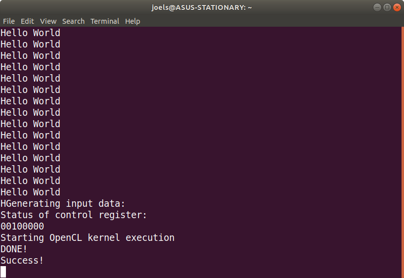
print("Generating input data: \n\r");
for (i = 0; i < WG_SIZE_X; i ++) {
a[i] = 1;
b[i] = 2;
c[i] = 0;
}
Xil_DCacheFlush();
*a_addr = (unsigned int)a;
*b_addr = (unsigned int)b;
*c_addr = (unsigned int)c;
/* set the workgroup identity */
*wg_y = 0;
*wg_z = 0;
*wg_x = 0;
*o_x = 0;
*o_y = 0;
*o_z = 0;
print("Status of control register: \n\r");
unsigned int con = *control;
for (i = 0; i < 8; i ++) {
if (con & (1 << i) ) {
print("1");
} else {
print("0");
}
}
print("\n\r");
print("Starting OpenCL kernel execution\n\r");
*control = *control | 1; /* start */
/* waiting for hardware to report "done" */
while (! ((*control) & 2));
print("DONE!\n\r");
Xil_DCacheInvalidate();
for (i = 0; i < WG_SIZE_X; i ++) {
if (c[i] != 3) ok = 0;
}
if (ok) {
print("Success!\n\r");
} else {
print("Error: Something went wrong!\n\r");
}
cleanup_platform();
return 0;
}
Now build (ctrl + b) and start up a debug session just like in the example with the hello world loop.
The output I capture on my screen sessions looks like this. Which seems to indicate a success.
C Code Walkthrough
This section goes through the C code step by step and offers some thoughts for each block. In this revised document I am, for now, leaving this unchanged but will go through it soon and see if there are things that can be better explained. I am just refreshing this knowledge myself, so I am far from expert in this area.
The code starts out by including some headers. This is just shown here for completeness.
#include <stdlib.h>
#include "platform.h"

#include "xil_io.h"
#include "xil_mmu.h"
#include "xil_cache.h"
#include "xil_cache_l.h"
The code below, declares names for the programming registers. The base address was for this was found in address edition in Vivado and the offsets to each specific register is found in the VHDL code generated from Vivado HLS.
volatile char *control = (volatile char*)0x43C00000;

volatile int *wg_x   = (volatile int*)0x43C00010;
volatile int *wg_y   = (volatile int*)0x43C00018;
volatile int *wg_z   = (volatile int*)0x43C00020;
volatile int *o_x    = (volatile int*)0x43C00028;
volatile int *o_y    = (volatile int*)0x43C00030;
volatile int *o_z    = (volatile int*)0x43C00038;

volatile int *a_addr = (volatile int*)0x43C00040;
volatile int *b_addr = (volatile int*)0x43C00048;
volatile int *c_addr = (volatile int*)0x43C00050;
The workgroup size is 128 (in the x direction). This means that each “run” of the generated hardware will perform 128 element wise additions.
#define WG_SIZE_X 128
#define WG_SIZE_Y 1
#define WG_SIZE_Z 1
This also means that the smallest amount of additions we can perform using the vadd hardware is 128 and that we can only perform multiples of 128 additions by repeatedly launching work on the vadd hardware with different workgroup identities. This restriction comes the use of the “reqd_work_group_size(128,1,1)” attribute used in the implementation of vadd in vivado_hls. This attribute can be left out resulting in a more flexible (but less efficient) hardware implementation with a more complicated interface.
The main function starts out by performing some standard initialization but we also add a step that marks the range of memory containing the programming registers as “non cacheable”.
int main()
{
    init_platform();
    /* more initialization */
    Xil_SetTlbAttributes(0x43c00000,0x10c06);  /* non cacheable */
The following piece of code declares pointers and allocates memory for the input and output to the vadd computation. It also declares a counter variable i (used in some loops later on) and an ok status variable.
int *a;
    int *b;
    int *c;
    int i;
    int ok = 1;

    a = (int*)malloc(WG_SIZE_X *sizeof(int));
    b = (int*)malloc(WG_SIZE_X *sizeof(int));
    c = (int*)malloc(WG_SIZE_X *sizeof(int));
Generate some input data and flush the cache to ensure that all the data we generated has been stored all the way to DRAM before launching the vadd computation.
print("Generating input data: \n\r");
    for (i = 0; i < WG_SIZE_X; i ++) {
        a[i] = 1;
        b[i] = 2;
        c[i] = 0;
    }
    Xil_DCacheFlush();
The next step is to program the registers of the vadd unit and prepare for launching a workgroup. The workgroup id is set to (0,0,0).
*a_addr = (unsigned int)a;
    *b_addr = (unsigned int)b;
    *c_addr = (unsigned int)c;

    /* set the workgroup identity */
    *wg_y = 0;
    *wg_z = 0;
    *wg_x = 0;

    *o_x = 0;
    *o_y = 0;
    *o_z = 0;
The next piece of code prints the contents of the control register. This serves no important purpose for the application but only provides a way to visually inspect that the control status (which should be “idle”).
print("Status of control register: \n\r");
    unsigned int con = *control;
    for (i = 0; i < 8; i ++) {
        if (con & (1  << i) ) {
            print("1");
        } else {
            print("0");
        }
    }
    print("\n\r");
We instruct the vadd hardware to start computing by putting a one at bit position zero in the control register.
print("Starting OpenCL kernel execution\n\r");
    *control = *control | 1;  /* start */
And then we wait for the hardware to report done in bit position two.
/* waiting for hardware to report "done" */
    while (! ((*control) & 2));
    print("DONE!\n\r");


    Xil_DCacheInvalidate();
After the hardware reports to be done, we invalidate the cache of the processing system in order to ensure that we will see the fresh data that the programmable logic has computed (without any involvement of the cache hierarchy, so the changes in memory are not yet visible to the ARM cores).
After that we can check the result for correctness.
for (i = 0; i < WG_SIZE_X; i ++) {
        if (c[i] != 3) ok = 0;
    }

    if (ok) {
        print("Success!\n\r");
    } else {
        print("Error: Something went wrong!\n\r");
    }
And we are done.
cleanup_platform();
    return 0;
}
Conclusion
Phew! I am actually quite surprised that this worked at all. It is quite a spaghetti like process to go through that interfaces 3 different GUIs and lots of steps in each! It would be nice to learn some more about how to script all these steps using TCL.
I hope this guide helps you in taking your first steps on the Zynq using OpenCL. If you have constructive feedback on improvements on this information, please let me know.
Thanks for reading and have a great day!
Please contact me with questions, suggestions or feedback at blog (dot) joel (dot) svensson (at) gmail (dot) com or join the google group .
© Copyright 2020 Bo Joel Svensson
This page was generated using Pandoc.