 |
|  |
|When starting up the STM32F4-Discovery board (bare metal), it will not be configured to run at full potential. So in this post we will try to configure the MCU to run at 168MHz, which is what the STMF32F407 should be capable of. I noticed that the STM32F411 on the other hand maxes out at 100MHz, this is the MCU on my other discovery board. So, it is good to know if one has a STM32F407G-DISC1 or a STM32F411E-DISC0. I guess most of what we do here today will be in essence the same on all STM32F4 but the various speeds one can configure differ, so the details will be different on different boards.
I think that knowing the speed of MCU may be an important thing going onwards. Say for example we want to talk to some external device and there is a timing aspect to that interface. To handle such things we need to be able to set up some ways to perform delays of a known duration or perhaps to measure time. Anyway! this post will just be about that attempt on configuring the clock, saving the rest for later.
Now, a bit of a disclaimer, I am not an expert and you should not follow this as "THE WAY" to do things. This statement holds true for all my posts. I am just an enthusiast that experiments and shares my experiences in doing so.
The "research" used as a base for the code produced in this post comes from A LOT of reading in the reference manual together with LOADS of googling. Clock configuration seems to be a concept surrounded by a mist of mystique and there is a lot of confusing information out there. It feels like there is a lot of "the blind leading the blind" going on and unfortunately this post is no different. So please if you are an expert in this and you see a way to improve the presentation, all your hints tips and feedback will be much appreciated. If you are noob, like me, and trying this out on a board of your own, please share your experience as well. Together we learn more.
Page 260 of the reference manual shows the clock tree of the STM32F4. This picture shows generated clocks pointing towards the right side of the picture and more-of-like "IO" functionality along the left edge. The middle is full of MUXes and logic. It is this middle area that we are going to be configuring.
The code we will write is concerned mostly will the following concepts from the clock tree:
N and P, Q and R divisors. There is also a divisor on the input to the PLL, called M. The input to the PLL is either HSI or HSE.SWSW-MUX and the AHB prescaler there the note "SYSCLK".Non-essential, but very helpful for debugging, is to also look at the following concept.
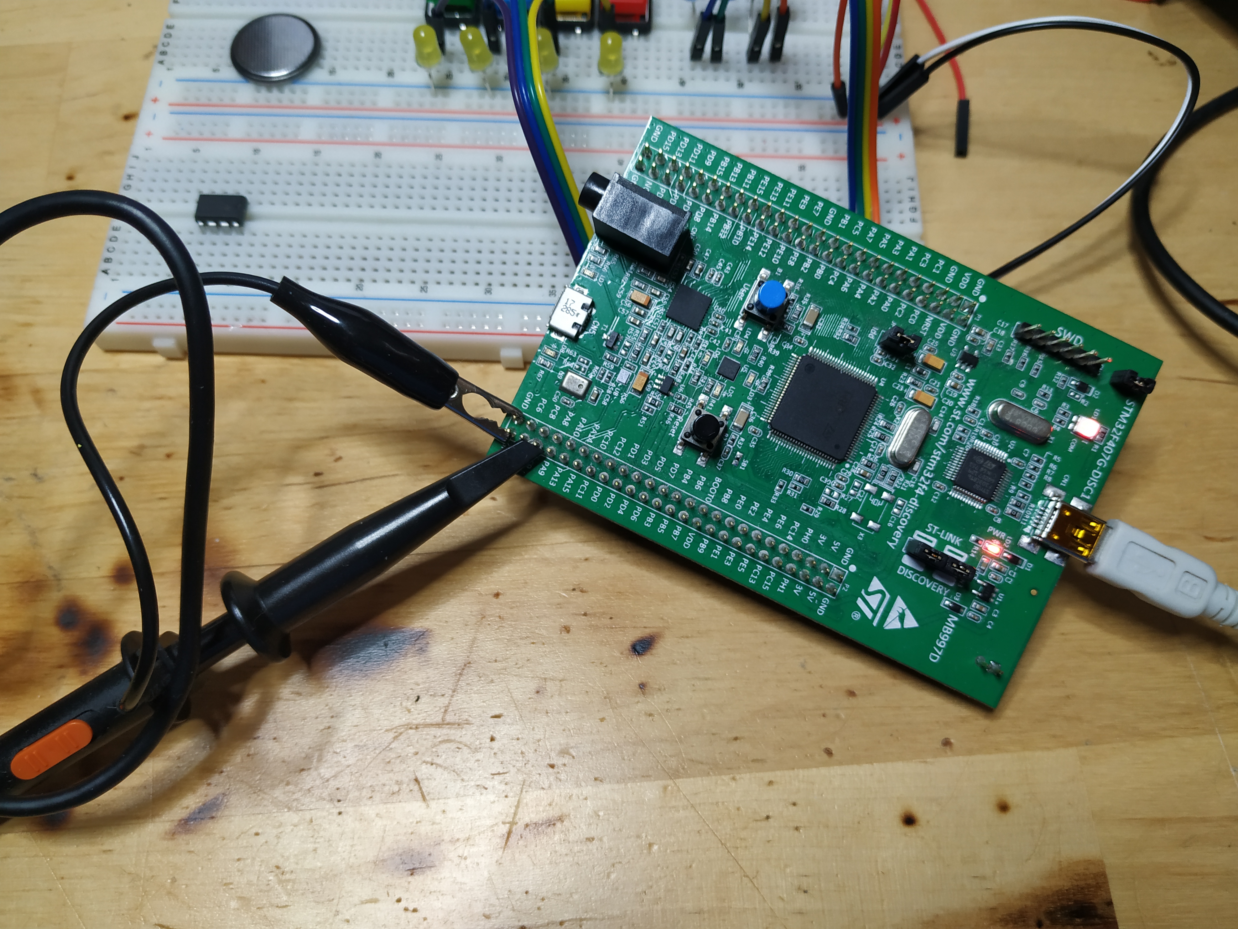
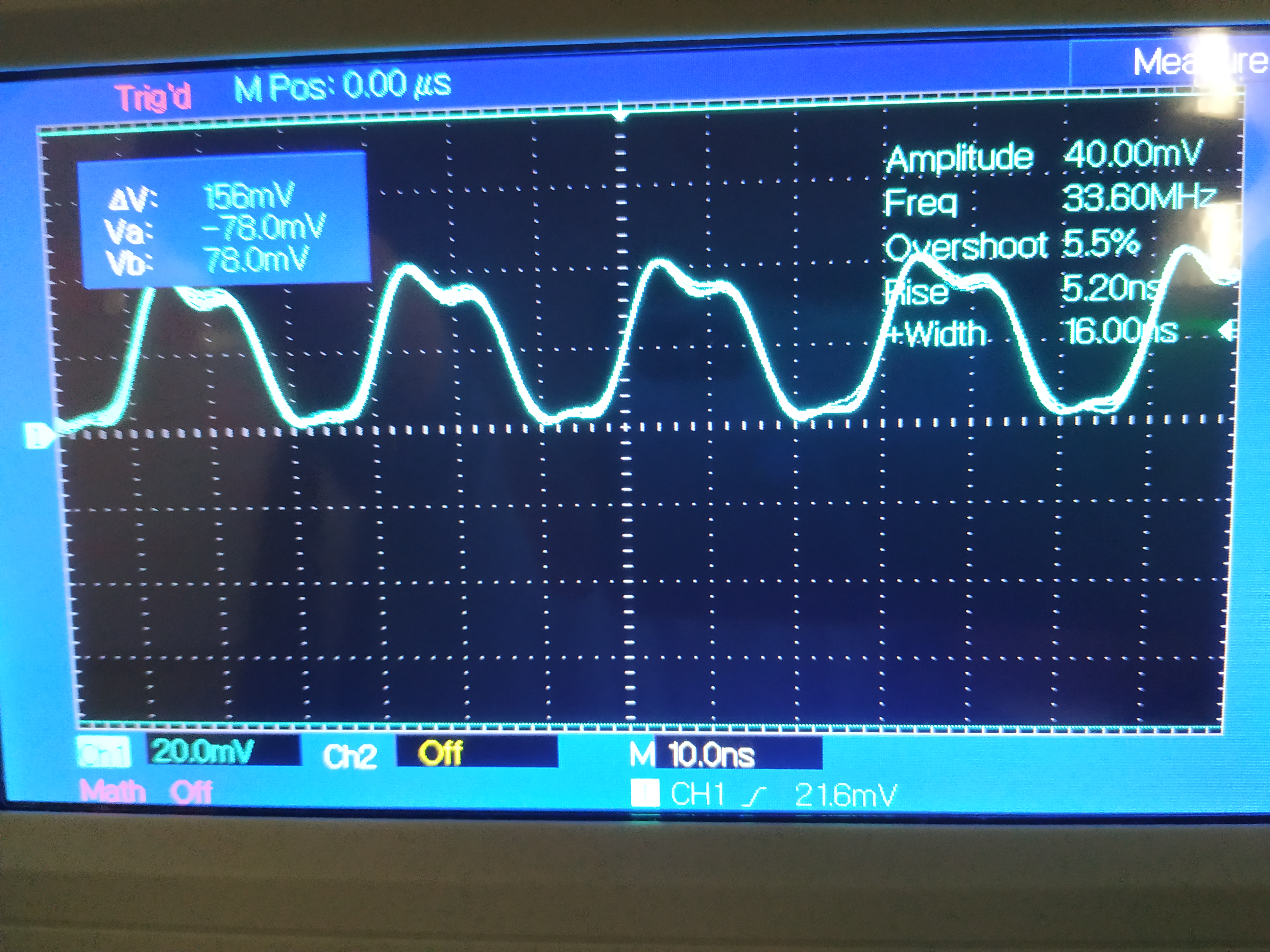
| Probed discovery board | Oscilloscope showing MCO2 signal | | ---- | ---- | | | |
So the goal here is to get the PLL to generate a 168MHz clock and to use the external crystal (HSE) as the input clock. A goal on the side is to also generate a 48Mhz clock (the PLL48CK in the clock tree picture as I understand it). This 48MHz clock is needed for USB for example. My understanding of those aspects is quite vague at the moment and we probably wont try to use USB anytime soon.
Involved in configuring this clock setup are the registered listed below.
We will also make use of registers:
RCC_CR is used to turn HSE and PLL on and also to poll their state. RCC_CFGR holds configuration information related to the AHB, APB1 and APB2 prescalers as well MCO configuration and status and control signals for the MUX controlled by the SW signals. RCC_PLLCFGR is where you can set the multiplier and divisor ratios for the PLL as well as selecting the input source of the PLL. To make all these registers a bit easier to work with let's define some constants.
.equ directive and some equatesThe .equ directive is used to define a name for a constant that you can later refer to in the assembler code. In earlier posts in this series we have seen code such as this:
ldr r0, =0x40020000with an .equ we can make code like that much more readable.
        .equ GPIOA_MODER, 0x40020000

        ...

        ldr r0, =GPIOA_MODER
The memory footprint and the cost of executing the two programs above are exactly the same. The benefit, however, is that the code is slightly more readable and somewhat self-documenting.
So to start out, the following .equ declarations can be used to set up nice names for all the registers we will access.
        @ Register addresses
        .equ FLASH_ACR,   0x40023c00      @ FLASH Access Control Register
        .equ RCC_CR,      0x40023800      @ Clock Control Register
        .equ RCC_CFGR,    0x40023808      @ Clock Configuration Register
        .equ RCC_PLLCFGR, 0x40023804      @ PLL Configuration Register

        .equ RCC_AHB1ENR, 0x40023830      @ AHB1 Peripheral Clock Enable Register

        .equ GPIOA_MODER, 0x40020000      @ PA Mode Register
        .equ GPIOA_OUT,   0x40020014      @ PA Output Data Register
        .equ GPIOC_MODER, 0x40020800      @ PC Mode Register
        .equ GPIOC_AFRH,  0x40020824      @ GPIOC Alternate function register (high)
I also set up a bunch of .equs for some bit positions and a bit mask that will be used.
        @ Bits and Masks
        .equ RCC_PLLCFGR_RESET_KEEP_MASK, 0xF0BC8000     @ Bits that should be kept at reset value

        .equ RCC_CR_PLL_ENABLE_BIT, 0x01000000     @ PLL enable bit
        .equ RCC_CR_PLL_RDY_BIT,    0x02000000     @ PLL rdy bit

        .equ RCC_CR_HSE_ON_BIT,     0x00010000     @ HSE_ON bit
        .equ RCC_CR_HSE_RDY_BIT,    0x00020000     @ HSE_RDY flag

        @ Constants
        .equ DELAY_LOOP_ITERATIONS, 20000000
The reference manual states that in the RCC_PLLCFGR there are a bunch of "reserved" bits that should not be altered. The RCC_PLLCFGR_RESET_KEEP_MASK has a 1-bit on all of the locations of those "reserved" bits. This mask can be used to clear all the bits that we are allowed to change in the RCC_PLLCFGR register.
Then there are some .equs with a 1-bit at the location of an enable or ready bit in the RCC_CR register. These will be used to turn on HSE, PLL and to poll for their respective ready state.
Lastly an .equ that defines a name for the otherwise magical number representing the number of cycles to spend in a delay loop. The delay loop is only used in the code to blink a set of LEDs, it is not essential to the clock configuration.
Step 5, to configure the PLL for 168MHz and PLL48CK for 48MHz is done by setting values N, M, Q and P. M divides the input clock signal and the reference manual states that the input the PLL should be 1 - 2MHz. The external crystal on the discovery board is 8MHz, so to get 1MHz we should divide by 8. So let's do M = 8. The next interesting bit is that P divides the output from the PLL and this P value can only be set to 2,4,6 or 8. That is, there is no option to not divide the output. This means that the N value must be set to 336 to get a 168MHz clock out of the PLL with input div M = 8. So this sets up the PLL clock signal frequency as (8 / 8) * 336 / 2 = 168MHz. The PLL48CK clock, now, has to be derived from that 336MHz, this can be done by a division by 7 so PLLQ will be set to 7.
Another way to set the up the PLL would be like this, (8 / 4) * 168 / 2 = 168MHz but then there would be no way to obtain the PLL48CK clock since 168 / 48 = 3.5. The reference manual states that it would be better to have an input frequency of 2MHz to the PLL, but with that input clock it is not possible to run the SYSCLK at 168MHz and the PLL48CK at 48MHz.
Now I think we should jump in the code!
As usual a lot of the code is similar to the code written in the previous post in the series. So let's jump directly to the point where the new stuff happens. Also, the complete source code will be given in full further down. Assume that we have all the .equs from the previous section.
The clock configuration code is run in the reset_handler right after a label called reset_continue.
reset_continue:
        @ Try some clock stuff

        ldr r0, =FLASH_ACR
        ldr r1, [r0]            @ should be zeroes after reset
        ldr r2, =0x705
        orr r1, r1, r2          @ 5 wait states
        str r1, [r0]
Just like "the plan" stated we start out by tweaking the FLASH settings. The code above sets the bits 0 - 3 to the value 5 (5 wait states) and the bits 8, 9 and 10 are each set to one, this corresponds to the value 0x705 loaded into r2 above. Bits 8,9 and 10 enables instruction cache, data cache and prefetch.
The reference manual claims that the "reset value" of the FLASH_ACR register is 0 (that is, all zeroes) as I understand it. As this code is the first thing we do to FLASH_ACR I assume it to be zero and there is no need to clear any bits before oring in the new values.
Next we load the address of RCC_CFGR into r0 and starts to build a value in r2 that we can or into that register.
        @ RCC_CFGR
        ldr r0, =RCC_CFGR
        mov r1, 0

    @ Output sysclk onto PC9 (MCO2) for debugging
        mov r2, 0x7             @ Divide by 5
        lsl r2, r2, 27          @ MCO2
        orr r1, r1, r2
The first part sets the MCO2 settings to output SYSCLK / 5. The shift left by 27 bits comes from the reference manual and points out where the bits of the RCC_CFGR that correspond to MCO2 are.
        mov r2, 0x5             @ PPRE1 (DIV 4)
        lsl r2, 10
        orr r1, r1, r2

        mov r2, 0x4             @ PPRE0 (DIV 2)
        lsl r2, 13
        orr r1, r1, r2

        str r1, [r0]
Then PPRE0 and PPRE1 configuration values are set. These are those prescalers related to APB1 and APB2 we talked about earlier.
The AHB prescaler will be set to 0x0, that is we wont put any value at all into RCC_CFGR related to that and thus there is no code above to deal with that aspect.
The str r1, [r0] instruction writes the settings we have created in r1 back into the RCC_CFGR register.
By now we have performed also step 2 and 3 of "the plan".
Next in line is to turn on the HSE and this is done by writing a bit into the RCC_CR register.
After writing the HSE_ON bit we should wait until a HSE_RDY flag turns on.
        @ RCC_CR ** TURN on HSE
        ldr r0, =RCC_CR
        ldr r1, [r0]

        ldr r2, =RCC_CR_HSE_ON_BIT
        orr r1, r1, r2
        str r1, [r0]

        @ Wait for HSE_RDY to be set
        ldr r2, =RCC_CR_HSE_RDY_BIT
wait_hse_rdy:
        ldr r1, [r0]            @ poll RCC_RC
        and r1, r1, r2
        cmp r1, r2
        bne wait_hse_rdy        @ loop if not rdy
The code above loads the contents of RCC_CR into r1 and then turns HSE on (sets a bit) and then writes r1 back to RCC_CR. Then a loop executes that poll the HSE_RDY bit in every iteration until it is set.
That concludes step 4.
So now it is time for step 5 where we actually set up for our 168MHz clock! This step starts out by loading RCC_PLLCFGR into r1 and then clears all bits that are not in the RESET_KEEP_MASK that we defined in the .equ section.
        @ PLLCFGR
        ldr r0, =RCC_PLLCFGR
        ldr r1, [r0]

        ldr r2, =RCC_PLLCFGR_RESET_KEEP_MASK
        and r1, r1, r2          @ Clear everything else

        mov r2, 336             @ multiplication factor
        lsl r2, r2, 6           @ PLLN
        orr r1, r1, r2

        mov r2, 8               @ division on input (PLLM)
        orr r1, r1, r2

        mov r2, 7               @ Division factor usb
        lsl r2, r2, 24          @ PLLQ
        orr r1, r1, r2

        mov r2, 1
        lsl r2, r2, 22          @ HSE source for pll
        orr r1, r1, r2

        str r1, [r0]
The code above set the N, M, Q and P factors as derived in "the plan" section. The P factor is going to be set to 0, so there is no code for that explicitly here. Those P bits are already cleared as a result of the initial clearing of all non-keep bits. The shift values used (lsl instructions) can all be found in the reference manual.
In the code above the HSE is also set as the source for the PLL, just before storing the new configuration back into the RCC_PLLCFGR register.
That is the end of step 5.
The next step should enable the PLL in a process very similar to how we started the HSE.
        ldr r0, =RCC_CR
        ldr r1, [r0]

        ldr r2, =RCC_CR_PLL_ENABLE_BIT
        orr r1, r1, r2
        str r1, [r0]

        @ Wait for PLL_RDY flag to be set
        ldr r2, =RCC_CR_PLL_RDY_BIT
wait_pll_rdy:
        ldr r1, [r0]
        and r1, r1, r2
        cmp r1, r2
        bne wait_pll_rdy
The code above loads the RCC_CR into r1 and then sets the bit that enables the PLL. After setting the enable pin we go into loop that polls the PLL_RDY bit.
That finishes off step 6.
Last step. In RCC_CFGR there are two bits that sets what to use the source of the SYSCLK. This is that very central MUX of the clock tree, the one with the SW control input. After setting a value on the SW control we should wait until that pattern is duplicated on another pair of pins and that is what the code below should be doing.
        @ Set PLL as source for sysclk
        ldr r0, =RCC_CFGR
        ldr r1, [r0]
        orr r1, r1, 0x2         @ PLL as source for SYSCLK
        str r1, [r0]

        @ Wait for sw flags to indicate PLL is used for SYSCLK
wait_use_pll:
        ldr r1, [r0]
        and r1, r1, 0xC         @ System clock switch status bits
        cmp r1, 0x8             @ Is PLL used as SYSCLK?
        bne wait_use_pll
Phew! Very obscure but there it is. At least my understanding of "it", is there.
Lastly, we should also configure PC 9 to use alternative function 0. This is done by first enabling GPIO C in the RCC_AHB1ENR register then setting up the GPIOC_MODER register so that PC9 is set to use alternatice function. Following that one should make sure that the GPIOC_AFRH is set so that PC9 is configured for alternative function 0. The alternative function is described using 4 bits, this is why there is a LOW and a HIGH alternative function register, just because a single 32bit register cannot hold 4 configuration bits for all 16 of GPIOC pins.
main:
        ldr r1, =RCC_AHB1ENR
        ldr r0, [r1]
        orr r0, 0x1             @ Turn on GPIO A
        orr r0, 0x4             @ Turn on GPIO C
        str r0, [r1]            @ Make it happen

        ldr r0, =GPIOC_MODER    @ PC9 alternative function mode
        ldr r1, [r0]
        ldr r2, =0xFFF3FFFF
        and r1, r1, r2
        mov r2, 2
        lsl r2, 18
        orr r1, r1 ,r2
        str r1, [r0]

        ldr r0, =GPIOC_AFRH     @ PC9 alternative function 0
        ldr r1, [r0]
        ldr r2, =0xFFFFFFF0F
        and r1, r1, r2
        str r1, [r0]
I placed this configuration of GPIOC following the "main" label.
Below you can find the complete assembly code listing:
        .syntax unified
        .cpu cortex-m4
        .thumb

        .global vtable
        .global reset_handler

        .section .text

        @ Register addresses
        .equ FLASH_ACR,   0x40023c00      @ FLASH Access Control Register
        .equ RCC_CR,      0x40023800      @ Clock Control Register
        .equ RCC_CFGR,    0x40023808      @ Clock Configuration Register
        .equ RCC_PLLCFGR, 0x40023804      @ PLL Configuration Register

        .equ RCC_AHB1ENR, 0x40023830      @ AHB1 Peripheral Clock Enable Register

        .equ GPIOA_MODER, 0x40020000      @ PA Mode Register
        .equ GPIOA_OUT,   0x40020014      @ PA Output Data Register
        .equ GPIOC_MODER, 0x40020800      @ PC Mode Register
        .equ GPIOC_AFRH,  0x40020824      @ GPIOC Alternate function register (high)

        @ Bits and Masks
        .equ RCC_PLLCFGR_RESET_KEEP_MASK, 0xF0BC8000     @ Bits that should be kept at reset value

        .equ RCC_CR_PLL_ENABLE_BIT, 0x01000000     @ PLL enable bit
        .equ RCC_CR_PLL_RDY_BIT,    0x02000000     @ PLL rdy bit

        .equ RCC_CR_HSE_ON_BIT,     0x00010000     @ HSE_ON bit
        .equ RCC_CR_HSE_RDY_BIT,    0x00020000     @ HSE_RDY flag

        @ Constants
        .equ DELAY_LOOP_ITERATIONS, 20000000


vtable:
        .word _estack
        .word reset_handler
        .word 0
        .word hard_fault_handler


        .thumb_func
delay:
        ldr r0,=DELAY_LOOP_ITERATIONS
delay_loop:
        cmp r0, 0
        beq delay_done
        sub r0,r0, 1
        b delay_loop
delay_done:
        bx lr

        .thumb_func
hard_fault_handler:
        b hard_fault_handler

        .thumb_func
reset_handler:
        ldr r0, =_estack
        mov sp, r0

        ldr r0, =_dstart        @ Address to copy to
        ldr r1, =_dend

        sub r2,r1,r0
        cmp r2, 0
        beq reset_continue

        ldr r1, =_flash_dstart  @ Address to copy from

cpy_loop:
        ldrb r3, [r1]
        strb r3, [r0]

        add r1, r1, 1
        add r0, r0, 1

        sub r2, r2, 1
        cmp r2, 0
        bne cpy_loop


reset_continue:
        @ Try some clock stuff

        ldr r0, =FLASH_ACR
        ldr r1, [r0]            @ should be zeroes after reset
        ldr r2, =0x105
        orr r1, r1, r2          @ 5 wait states
        str r1, [r0]

        @ RCC_CFGR
        ldr r0, =RCC_CFGR
        mov r1, 0

    @ Output sysclk onto PC9 (MCO2) for debugging
        mov r2, 0x7             @ Divide by 5
        lsl r2, r2, 27          @ MCO2
        orr r1, r1, r2

        mov r2, 0x5             @ PPRE1 (DIV 4)
        lsl r2, 10
        orr r1, r1, r2

        mov r2, 0x4             @ PPRE0 (DIV 2)
        lsl r2, 13
        orr r1, r1, r2

        str r1, [r0]

        @ RCC_CR ** TURN on HSE
        ldr r0, =RCC_CR
        ldr r1, [r0]

        ldr r2, =RCC_CR_HSE_ON_BIT
        orr r1, r1, r2
        str r1, [r0]

        @ Wait for HSE_RDY to be set
        ldr r2, =RCC_CR_HSE_RDY_BIT
wait_hse_rdy:
        ldr r1, [r0]            @ poll RCC_RC
        and r1, r1, r2
        cmp r1, r2
        bne wait_hse_rdy        @ loop if not rdy


        @ PLLCFGR
        ldr r0, =RCC_PLLCFGR
        ldr r1, [r0]

        ldr r2, =RCC_PLLCFGR_RESET_KEEP_MASK
        and r1, r1, r2          @ Clear everything else

        mov r2, 336             @ multiplication factor
        lsl r2, r2, 6           @ PLLN
        orr r1, r1, r2

        mov r2, 8               @ division on input (PLLM)
        orr r1, r1, r2

        mov r2, 7               @ Division factor usb
        lsl r2, r2, 24          @ PLLQ
        orr r1, r1, r2

        @ PLLP  (set to 00 gives div by 2)
        @ldr r2, =0xFFFCFFFF
        @and r1, r1, r2

        mov r2, 1
        lsl r2, r2, 22          @ HSE source for pll
        orr r1, r1, r2

        str r1, [r0]

        ldr r0, =RCC_CR
        ldr r1, [r0]

        ldr r2, =RCC_CR_PLL_ENABLE_BIT
        orr r1, r1, r2
        str r1, [r0]

        @ Wait for PLL_RDY flag to be set
        ldr r2, =RCC_CR_PLL_RDY_BIT
wait_pll_rdy:
        ldr r1, [r0]
        and r1, r1, r2
        cmp r1, r2
        bne wait_pll_rdy

        @ Set PLL as source for sysclk
        ldr r0, =RCC_CFGR
        ldr r1, [r0]
        orr r1, r1, 0x2         @ PLL as source for SYSCLK
        str r1, [r0]

        @ Wait for sw flags to indicate PLL is used for SYSCLK
wait_use_pll:
        ldr r1, [r0]
        and r1, r1, 0xC         @ System clock switch status bits
        cmp r1, 0x8             @ Is PLL used as SYSCLK?
        bne wait_use_pll


main:
        ldr r1, =RCC_AHB1ENR
        ldr r0, [r1]
        orr r0, 0x1             @ Turn on GPIO A
        orr r0, 0x4             @ Turn on GPIO C
        str r0, [r1]            @ Make it happen


        ldr r0, =GPIOC_MODER    @ PC9 alternative function mode
        ldr r1, [r0]
        ldr r2, =0xFFF3FFFF
        and r1, r1, r2
        mov r2, 2
        lsl r2, 18
        orr r1, r1 ,r2
        str r1, [r0]

        ldr r0, =GPIOC_AFRH     @ PC9 alternative function 0
        ldr r1, [r0]
        ldr r2, =0xFFFFFFF0F
        and r1, r1, r2
        str r1, [r0]

        ldr r1, =GPIOA_MODER
        ldr r0, [r1]            @ Value of PA MODER
        ldr r2, =0xFFFFFF00
        and r0, r0, r2
        orr r0, r0, 0x55        @ PA0 - PA 3 output,
        str r0, [r1]            @ Write back PA MODER


        ldr r3,=GPIOA_OUT
        ldr r5,=0xFFFFFF00      @ Clear-mask for bits of interest

        mov r1, 0xF
        mov r2, 0x0
forever:
        bl delay
        str r2, [r3]
        bl delay
        str r1, [r3]
b foreverFun stuff! I am pretty sure my MCU now runs at 168 MHz given that the oscilloscope output reads 33.6Mhz and 33.6 * 5 = 168. Remember that the MCO2 divisor was set to 5. Of course, the AHB, APB1 and APB2 are still a bit mysterious but once we need to understand that I am sure we can make it happen.
Writing assembly is quite annoying, very error prone and very tedious. So, I hope to look at the following things soon so that we can build some abstractions.
Now that we know how fast our MCU is going it would also be nice to try to come up with some more clever ways of doing delays. Would also be fun to see if we can set up a regularly occurring interrupt and fire off some interesting code every N time units.
The code is available at GitHub.
Thanks a lot for reading. I hope you are well and have a good day. As usual I would love to hear feedback, hints, tips, your experience... yeah anything. Be well!
Please contact me with questions, suggestions or feedback at blog (dot) joel (dot) svensson (at) gmail (dot) com or join the google group .
© Copyright 2021 Bo Joel Svensson
This page was generated using Pandoc.