It is always rewarding to be able to get some visual feedback when implementing stuff. So getting the VGA port on the nexys a7 to work has been high on the wish-list.
This text describes my attempt at getting some VGA graphics to display. I am not entirely happy with it but it does display things. I was going for a resolution of 640x400 but the screens I have available all detect the signal as 720x400. This may not be that bad, we'll see. So anyway, if 640x400 really is no-go, then we can later re-purpose it for 640x480 and just not plot anything on 80 of the lines.
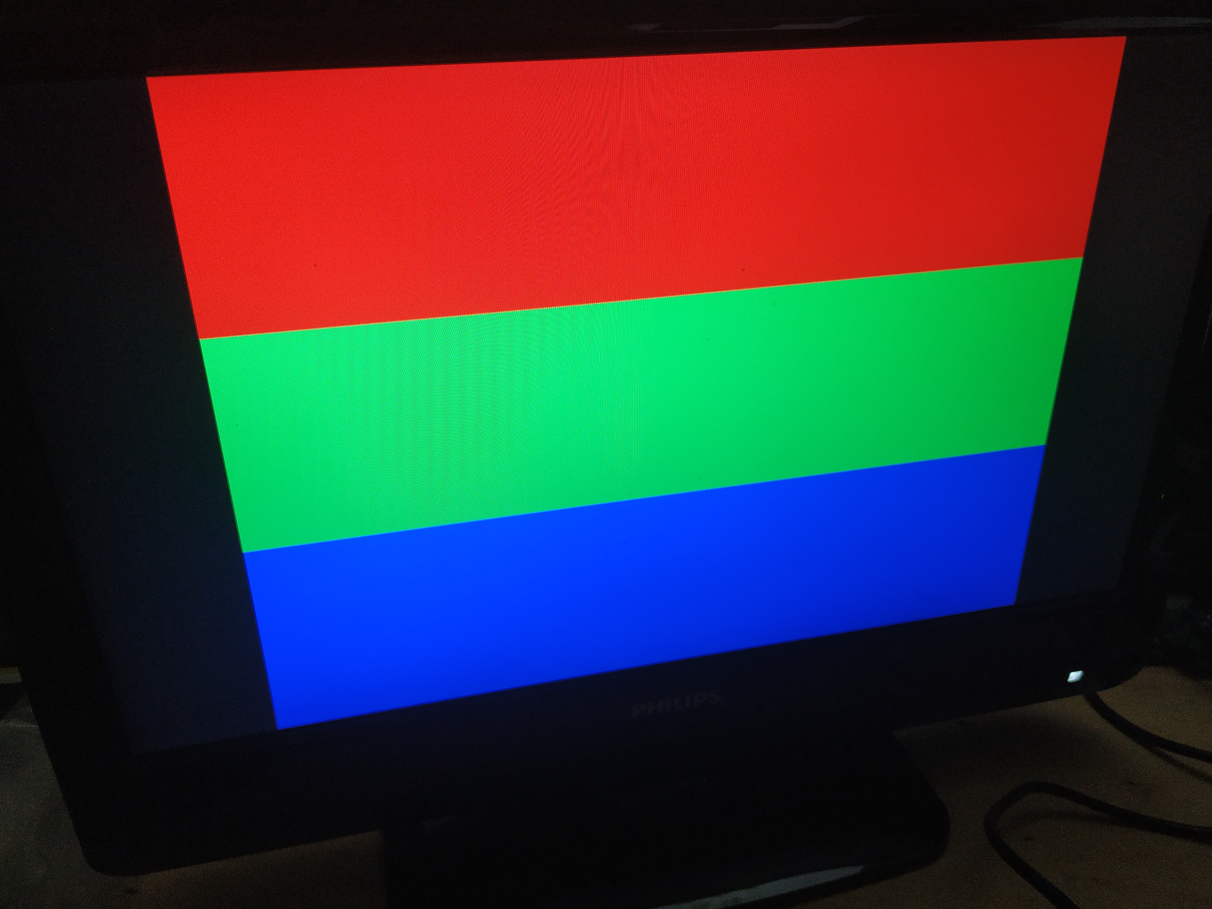
Before jumping into the implementation of this stuff, here are some pictures of the result!
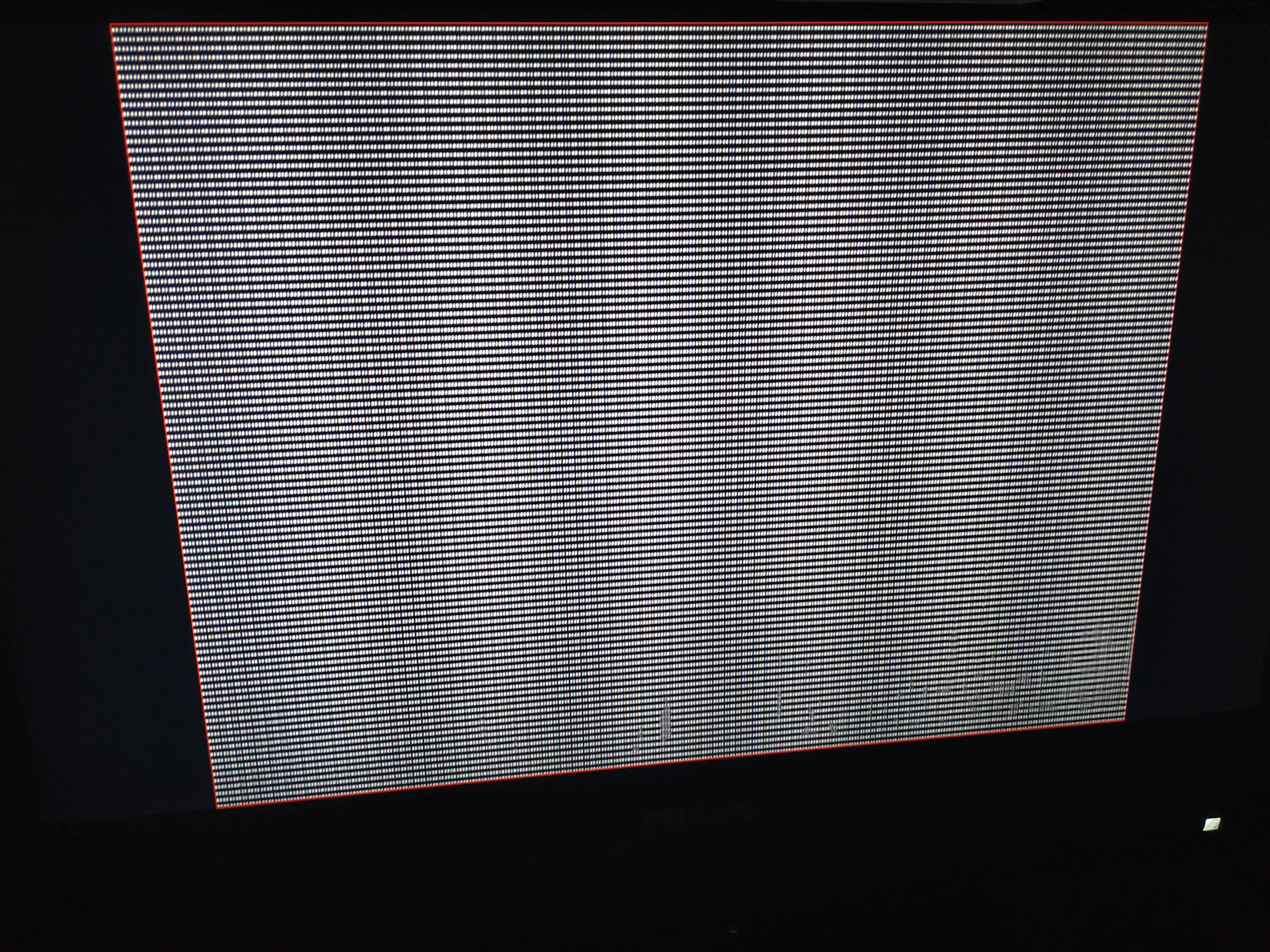
The pixels look very fuzzy as can be seen in the second of the picture. I am not sure why this is. There could be many reasons, the timing is not exact as the spec says, it is analog video and we are used to digital now, The TV is bad. If you know this stuff and can instantly tell, please let me know in an email.
I used the pixel-clock counts from this page as the basis for this implementation.
So, let's jump into it.
The signals involved in VGA are color (RGB), horizontal sync and vertical sync. Each of the R,G,B channels are made up of 4 bit bit-arrays. That R,G and B are 4 bit vectors is probably more related to how the physical interface is implemented on the FPGA (is my guess). Input signals to the VGA unit will be a clock and a reset signal.
So the entity declaration will look as follows:
entity vga is
    Port (
        vga_r : out std_logic_vector(3 downto 0);
        vga_g : out std_logic_vector(3 downto 0);
        vga_b : out std_logic_vector(3 downto 0);
        vga_hs : out std_logic;
        vga_vs : out std_logic;

        clk : in std_logic;
        reset : in std_logic

       -- clk_out : out std_logic;
       -- hcnt : out unsigned(10 downto 0);
       -- vcnt : out unsigned(10 downto 0)
    );
end vga;
I have a few lines that are commented out in the entity declaration. These are signals that I enabled when doing simulation to be able to look inside of the module and see what goes on with otherwise internal signals.
If we look at this page we can see that we need a 25.175 MHz pixel-clock. I will gamble that 25MHz is roughly ok as that can be derived from the 100MHz clock that I will try to synthesize for by dividing the clock frequency by 4. All the other timing information is then derived from this pixel-clock in given number of ticks.
The Horizontal timing for example consists of 640 clock ticks of visible data output, 16 ticks that should output blackness, followed by 96 ticks with the horizontal synch signal active, then another 48 ticks of blackness. That is a total of 800 ticks that then repeat over and over again.
The horizontal synch corresponds to when (in the old CRT days) the electron beam traced back across the screen to start on the next line.
For the vertical timing it works in very much the same way. One difference here is that the times are now expressed in multiples of full lines. so for one vertical "tick" to occur, 800 horizontal ones will have occurred.
The 25MHz pixel-clock is generated by first dividing the input clock clk of 100MHz by first 2 and then by 2 again. This is done using two processes.
    clk_div_2: process(clk, reset)
    begin
        if (reset = '1') then
            clk_2 <= '0';
        elsif rising_edge(clk) then
            clk_2 <= not clk_2;
        end if;
    end process;

    pix_clk_gen: process(clk_2, reset)
    begin
        if (reset = '1') then
            pix_clock <= '0';
        elsif rising_edge(clk_2) then
            pix_clock <= not pix_clock;
        end if;
    end process;
The clk_2 and the pix_clock signals are internal to the architecture and will represent a 50MHz and a 25MHz clock. I am actually not sure if there should be any reset for these processes, I almost assume it will work without any reset.
Two counters are used to keep track of the timing.
    signal h_cnt : unsigned(9 downto 0);
    signal v_cnt : unsigned(9 downto 0);
These counter will be updated in a control process and h_cnt will take on the values from 0 to and including 799. The v_cnt signal will take on the values from 0 to and including 448.
The HSYNCH and VSYNCH signals are generated outside of any process
    vga_hs <= '0' when h_cnt >= 656 and h_cnt < 752 else '1';
    vga_vs <= '1' when v_cnt = 412 or v_cnt = 413 else '0';
The value ranges used here are again found here. we can also see that the vertical sync signal is active high while the horizontal one is active low. I hope I got those right. This actually seems to vary between the different display modes! Some modes have vertical sync active high, other low and likewise horizontal sync may vary.
The control process is in charge of updating the h_cnt and v_cnt counters. For this test program, the color data is also output from this process. So if the h_cnt is less than 640 and the v_cnt is less then 400, then color data is fed to the pins.
The control process is sensitive to the pixel-clock at 25MHz. So this is where most of the timing takes place.
    control: process(pix_clock, reset)
    begin

        if (reset = '1') then
            h_cnt <= to_unsigned(0, h_cnt'length);
            v_cnt <= to_unsigned(0, v_cnt'length);
        elsif rising_edge(pix_clock) then

            if (h_cnt < 640 and v_cnt < 400) then
                if (h_cnt = 0 or v_cnt = 0 or
                    h_cnt = 639 or v_cnt = 399) then
                    vga_r <= X"F";
                    vga_g <= X"0";
                    vga_b <= X"0";
                elsif (h_cnt(0) = '1' and v_cnt(1) = '1') then
                    vga_r <= X"F";
                    vga_g <= X"F";
                    vga_b <= X"F";
                else
                    vga_r <= X"0";
                    vga_g <= X"F";
                    vga_b <= X"0";
                end if;
            else
                vga_r <= X"0";
                vga_g <= X"0";
                vga_b <= X"0";
            end if;

            if (h_cnt < 800) then
                h_cnt <= h_cnt + 1;
            else
                h_cnt <= to_unsigned(0, h_cnt'length);
                if (v_cnt < 449) then
                    v_cnt <= v_cnt + 1;
                else
                    v_cnt <= to_unsigned(0, v_cnt'length);
                end if;
            end if;
        end if;
end process;library IEEE;
use IEEE.STD_LOGIC_1164.ALL;
use IEEE.NUMERIC_STD.ALL;
entity vga is
Port (
vga_r : out std_logic_vector(3 downto 0);
vga_g : out std_logic_vector(3 downto 0);
vga_b : out std_logic_vector(3 downto 0);
vga_hs : out std_logic;
vga_vs : out std_logic;
clk : in std_logic;
reset : in std_logic
-- clk_out : out std_logic;
-- hcnt : out unsigned(10 downto 0);
-- vcnt : out unsigned(10 downto 0)
);
end vga;
architecture Behavioral of vga is
signal pix_clock : std_logic;
signal clk_2 : std_logic;
signal h_cnt : unsigned(9 downto 0);
signal v_cnt : unsigned(9 downto 0);
begin
--clk_out <= pix_clock;
--hcnt <= h_cnt;
--vcnt <= v_cnt;
clk_div_2: process(clk, reset)
begin
if (reset = '1') then
clk_2 <= '0';
elsif rising_edge(clk) then
clk_2 <= not clk_2;
end if;
end process;
pix_clk_gen: process(clk_2, reset)
begin
if (reset = '1') then
pix_clock <= '0';
elsif rising_edge(clk_2) then
pix_clock <= not pix_clock;
end if;
end process;
vga_hs <= '0' when h_cnt >= 656 and h_cnt < 752 else '1';
vga_vs <= '1' when v_cnt = 412 or v_cnt = 413 else '0';
control: process(pix_clock, reset)
begin
if (reset = '1') then
h_cnt <= to_unsigned(0, h_cnt'length);
v_cnt <= to_unsigned(0, v_cnt'length);
elsif rising_edge(pix_clock) then
if (h_cnt < 640 and v_cnt < 400) then
if (h_cnt = 0 or v_cnt = 0 or
h_cnt = 639 or v_cnt = 399) then
vga_r <= X"F";
vga_g <= X"0";
vga_b <= X"0";
elsif (h_cnt(0) = '1' and v_cnt(1) = '1') then
vga_r <= X"F";
vga_g <= X"F";
vga_b <= X"F";
else
vga_r <= X"0";
vga_g <= X"F";
vga_b <= X"0";
end if;
else
vga_r <= X"0";
vga_g <= X"0";
vga_b <= X"0";
end if;
if (h_cnt < 800) then
h_cnt <= h_cnt + 1;
else
h_cnt <= to_unsigned(0, h_cnt'length);
if (v_cnt < 449) then
v_cnt <= v_cnt + 1;
else
v_cnt <= to_unsigned(0, v_cnt'length);
end if;
end if;
end if;
end process;
end Behavioral;Edit Dec 1 2020
One thing I forgot to include here originally is the constraints file that connects the various signals the the VGA interface of the nexys a7 board.
set_property -dict {PACKAGE_PIN E3 IOSTANDARD LVCMOS33} [get_ports {clk}]
create_clock -period 10.000 -name sys_clk_pin -waveform {0.000 5.000} -add [get_ports {clk}]

##switch
set_property -dict {PACKAGE_PIN J15 IOSTANDARD LVCMOS33} [get_ports {reset}]

##VGA Connector
set_property -dict { PACKAGE_PIN A3    IOSTANDARD LVCMOS33 } [get_ports { vga_r[0] }]; #IO_L8N_T1_AD14N_35 Sch=vga_r[0]
set_property -dict { PACKAGE_PIN B4    IOSTANDARD LVCMOS33 } [get_ports { vga_r[1] }]; #IO_L7N_T1_AD6N_35 Sch=vga_r[1]
set_property -dict { PACKAGE_PIN C5    IOSTANDARD LVCMOS33 } [get_ports { vga_r[2] }]; #IO_L1N_T0_AD4N_35 Sch=vga_r[2]
set_property -dict { PACKAGE_PIN A4    IOSTANDARD LVCMOS33 } [get_ports { vga_r[3] }]; #IO_L8P_T1_AD14P_35 Sch=vga_r[3]
set_property -dict { PACKAGE_PIN C6    IOSTANDARD LVCMOS33 } [get_ports { vga_g[0] }]; #IO_L1P_T0_AD4P_35 Sch=vga_g[0]
set_property -dict { PACKAGE_PIN A5    IOSTANDARD LVCMOS33 } [get_ports { vga_g[1] }]; #IO_L3N_T0_DQS_AD5N_35 Sch=vga_g[1]
set_property -dict { PACKAGE_PIN B6    IOSTANDARD LVCMOS33 } [get_ports { vga_g[2] }]; #IO_L2N_T0_AD12N_35 Sch=vga_g[2]
set_property -dict { PACKAGE_PIN A6    IOSTANDARD LVCMOS33 } [get_ports { vga_g[3] }]; #IO_L3P_T0_DQS_AD5P_35 Sch=vga_g[3]
set_property -dict { PACKAGE_PIN B7    IOSTANDARD LVCMOS33 } [get_ports { vga_b[0] }]; #IO_L2P_T0_AD12P_35 Sch=vga_b[0]
set_property -dict { PACKAGE_PIN C7    IOSTANDARD LVCMOS33 } [get_ports { vga_b[1] }]; #IO_L4N_T0_35 Sch=vga_b[1]
set_property -dict { PACKAGE_PIN D7    IOSTANDARD LVCMOS33 } [get_ports { vga_b[2] }]; #IO_L6N_T0_VREF_35 Sch=vga_b[2]
set_property -dict { PACKAGE_PIN D8    IOSTANDARD LVCMOS33 } [get_ports { vga_b[3] }]; #IO_L4P_T0_35 Sch=vga_b[3]
set_property -dict { PACKAGE_PIN B11   IOSTANDARD LVCMOS33 } [get_ports { vga_hs }]; #IO_L4P_T0_15 Sch=vga_hs
set_property -dict { PACKAGE_PIN B12   IOSTANDARD LVCMOS33 } [get_ports { vga_vs }]; #IO_L3N_T0_DQS_AD1N_15 Sch=vga_vs
Sorry about that.
This file sets the desired clock to 100MHz which when divided by 4 will give the 25MHz pixel-clock. Then it connects up the various VGA signals to the correct pins on the package. The template for this comes from the "master" constraints file provided by the board manufacturer.
Thanks for reading. I hope it was informative in some way. If you have insights about this that I missed (very likely) or any suggestions of improvements, just let me know!
Thanks and have a good day.
Please contact me with questions, suggestions or feedback at blog (dot) joel (dot) svensson (at) gmail (dot) com or join the google group .
© Copyright 2020 Bo Joel Svensson
This page was generated using Pandoc.